
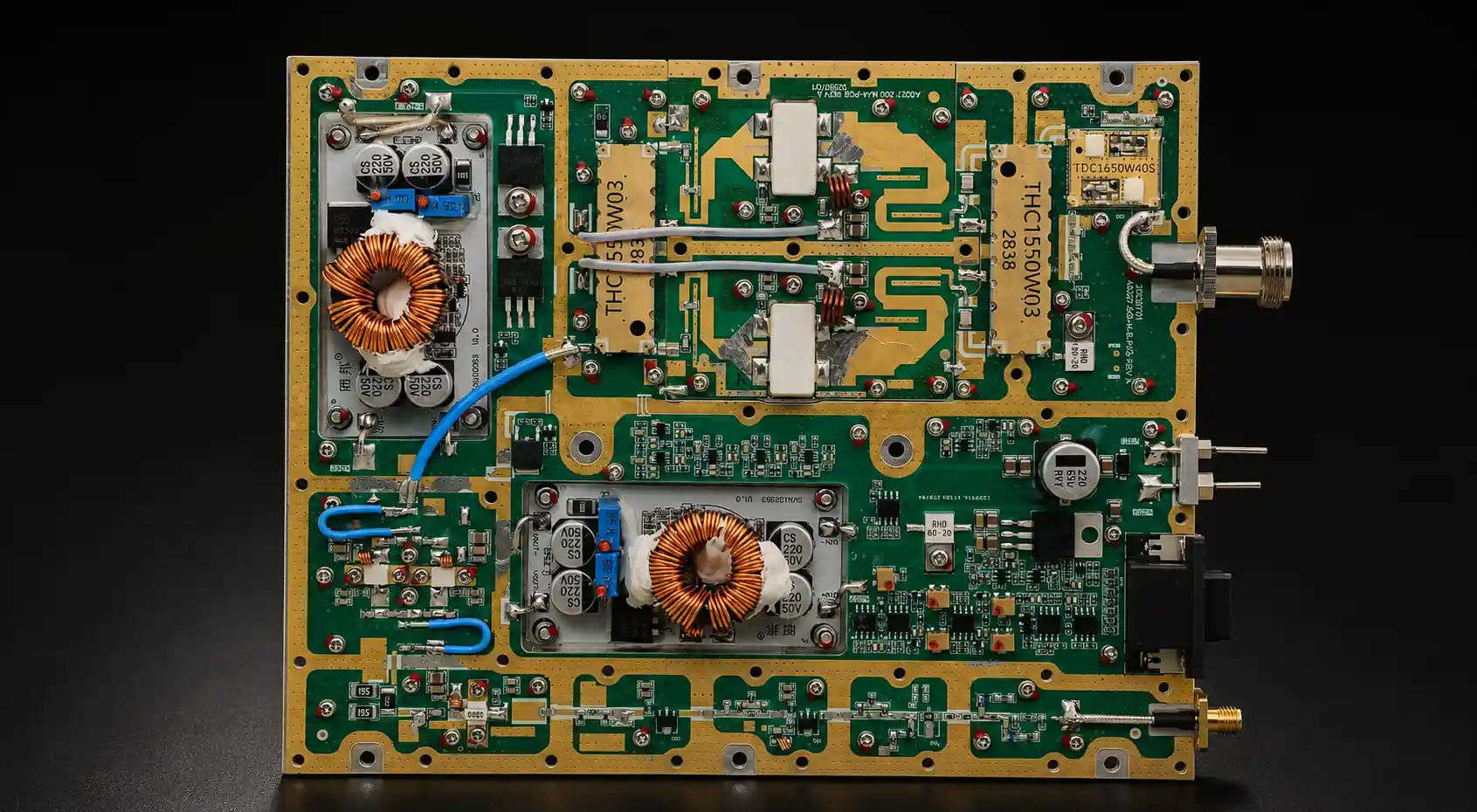
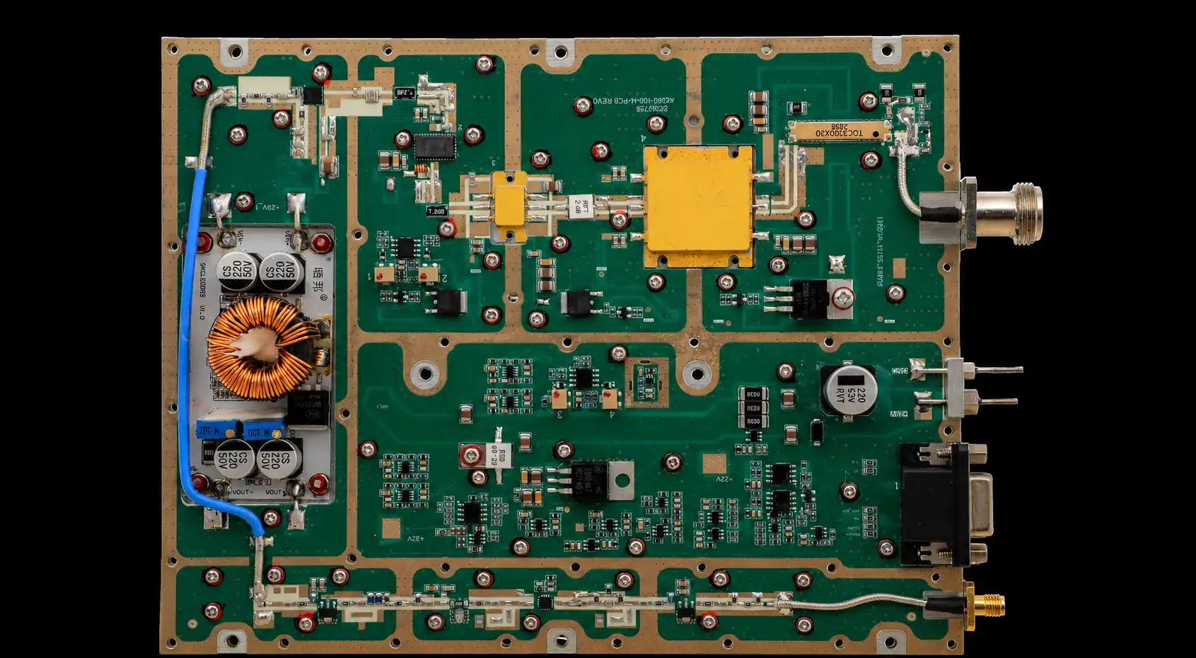
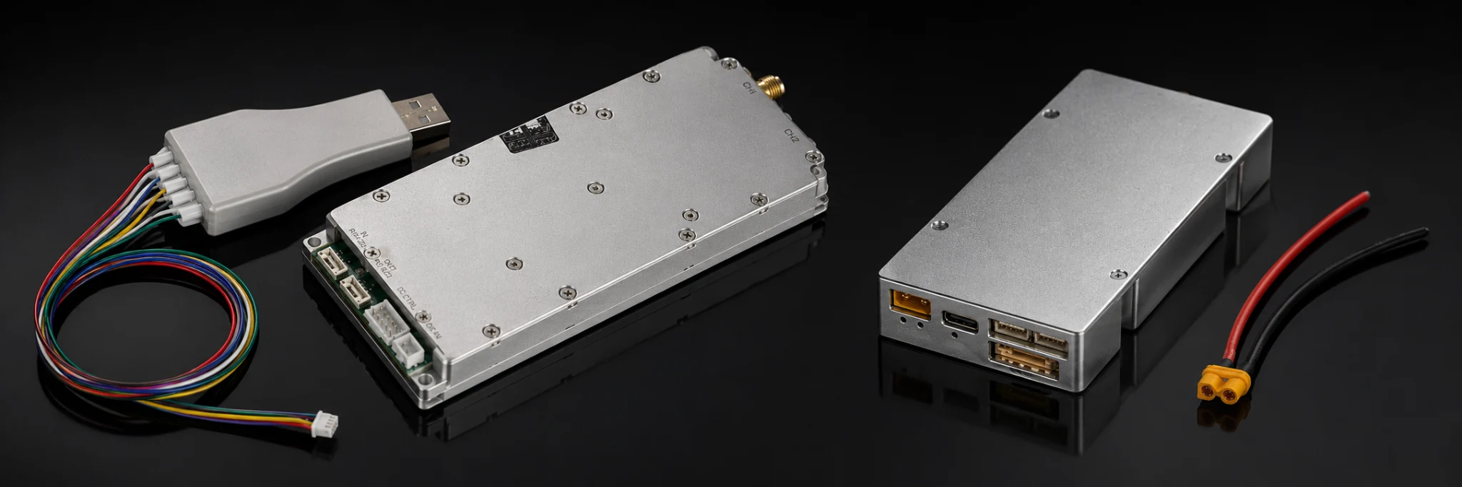
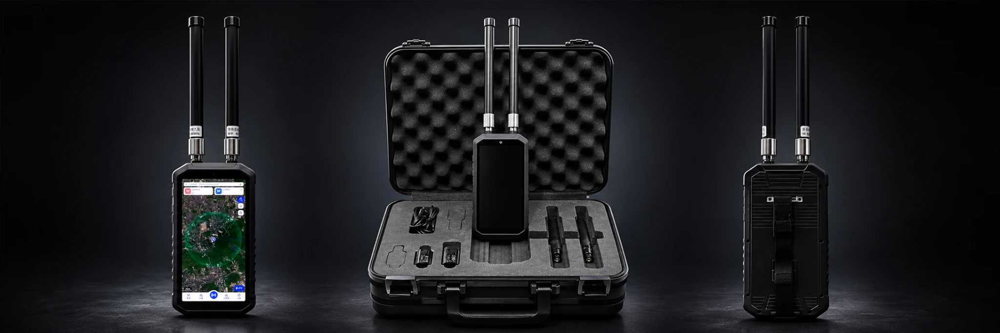


The GaN vs LDMOS RF amplifier decision has no universal winner across all applications. For a radio-frequency power amplifier (RF PA), GaN is often the stronger starting point when higher frequency, wide bandwidth, power density, and size, weight, and power (SWaP) dominate. LDMOS can remain the better fit when a qualified lower- or mid-band platform, reuse of existing electrical and mechanical assets, and total system cost dominate.
That comparison is meaningful only when both candidates are judged at the same operating boundary: frequency and bandwidth, output power (Pout) and its reference plane, actual input power (Pin), waveform, back-off, thermal state, cooling, load, supply, and evidence scope. A semiconductor label, one typical efficiency number, or one rated-power figure is not enough to choose a module.
The first decision is therefore simple: is the application defined well enough to compare the two technologies at all?
1. Start With the Application Boundary, Not the Semiconductor Label
Before comparing GaN and LDMOS, define the minimum project boundary:
- working frequency and instantaneous bandwidth;
- Pout as rated, minimum, typical, peak, or average power, at a defined reference plane;
- actual Pin at the PA input reference plane;
- waveform, duty cycle, peak-to-average ratio, linearity, and back-off;
- ambient and baseplate or case temperature;
- cooling method and available DC power;
- size, weight, load, VSWR, platform-reuse, and lifecycle constraints.
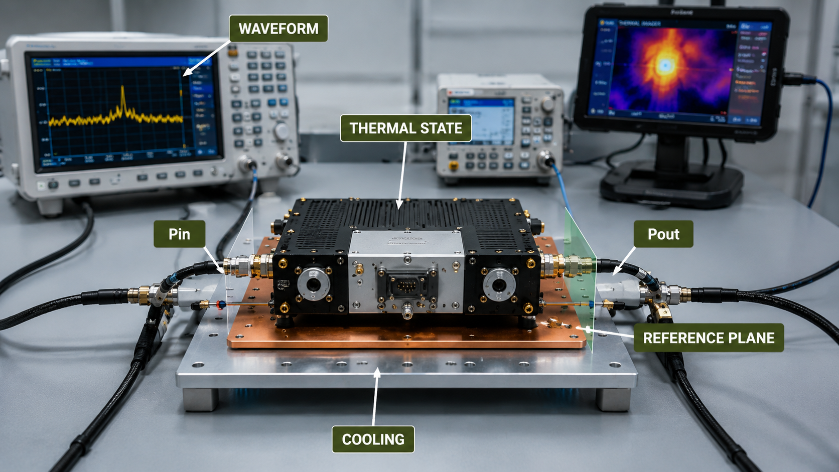
A reference plane is the physical point at which a power value applies. Comparing one amplifier at its output connector with another at a different system point is not a valid power comparison.
If frequency, Pout definition, reference plane, Pin, waveform, thermal state, or another route-changing condition is still unknown, the result is Not Comparable Yet. Record the missing condition instead of filling it with a typical assumption.
The output of this step is a minimum application-boundary record and one decision: proceed with technology comparison, or pause and complete the missing requirements. For a deeper requirements workflow, use the guide to define the RF PA application boundary.
2. What GaN and LDMOS Change Inside an RF Power Amplifier
GaN and LDMOS change the device-level design space. Depending on the selected device and operating frequency, they can influence frequency capability, gain, power density, operating voltage, optimum device impedance, and parasitic behavior.
Those differences affect amplifier architecture: matching, bias, driver requirements, packaging, grounding, combining, thermal design, and protection. The complete result then depends on how those elements are implemented.
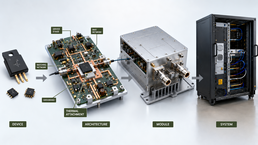
The useful reasoning chain is:
device-category trend → amplifier architecture → module implementation → system result
That distinction matters because a technology trend is not a module guarantee. Two amplifiers using the same transistor technology can still deliver different Pout, efficiency, linearity, thermal behavior, and mismatch response because the implementation is different.
When reviewing a performance claim, ask whether it describes a general technology trend or a measured result from a named device or module. The first can guide candidate selection; the second is required for a project-level conclusion. Packaging and transistor attachment can also change RF PA thermal performance, so a bare-device result cannot prove complete module behavior.
3. When GaN Is the Stronger Starting Point
GaN deserves higher validation priority when several constraints act together: higher-frequency operation, wide instantaneous bandwidth, multi-octave coverage, high RF output from limited board area, limited available drive power, or strict SWaP limits.
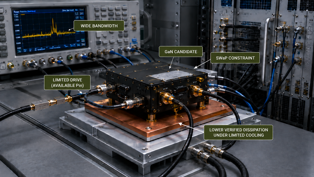
A higher device operating voltage can also change the current, power-supply, and matching design space, but whether that becomes a system advantage depends on the complete amplifier implementation.
Limited cooling volume may strengthen the case for a candidate with lower total dissipation at the required operating point. That still does not mean a compact GaN design is automatically easier to cool. High power density can concentrate heat around the transistor, package, attachment interface, and immediate heat spreader.
There is no universal frequency at which GaN automatically replaces LDMOS. The trigger is the combination of frequency, bandwidth, gain, Pin, Pout, mechanical limits, power supply, cooling, and evidence quality.
A Prioritize GaN decision should therefore mean: the application makes GaN the more valuable route to validate first, and the supplier must still provide module-level evidence for frequency coverage, Pout, Pin, waveform, linearity, efficiency, hot-state operation, cooling, and mechanical limits.
4. When LDMOS Is Still the Better Fit
LDMOS can remain the lower-risk route when the project benefits from an established platform. This is especially relevant in some lower- or mid-band, high-power, or narrowband applications where the supply, bias, matching, cooling, mechanical layout, production process, or qualification basis already exists.
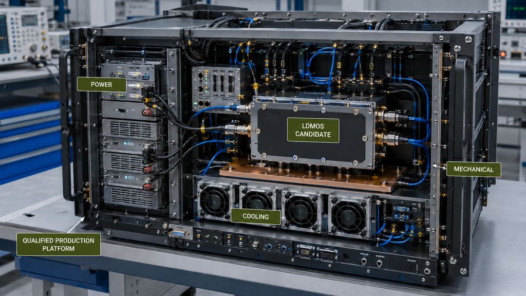
“Mature” should describe something specific: a device, module, platform, manufacturing process, or qualification state. It should not be used as a substitute for current product evidence.
The real question is what can be reused. If an LDMOS route preserves qualified power supplies, matching, thermal hardware, production processes, or certifications, while a technology change requires redesign and requalification, that difference may outweigh a device-level performance advantage.
A Prioritize LDMOS decision is justified only when the candidate still meets the same frequency, Pout, Pin, waveform, thermal, load, and interface requirements. Lifecycle and sourcing also require current evidence rather than assumptions about maturity; supplier stability and requalification risk should be reviewed separately from the material label.
5. Why GaN vs. LDMOS Is Not Always a Binary Choice
The technology decision can occur at different amplifier stages. A single-stage or multistage PA may use one technology throughout, but a complete architecture may also use different technologies in the driver and final stages.
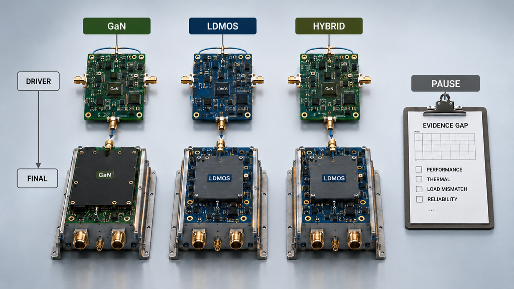
That creates four valid project outcomes:
Prioritize GaN — validate a GaN-based route first.
Prioritize LDMOS — validate an LDMOS-based route first.
Retain a hybrid architecture or dual-candidate route — keep more than one architecture open because stage-level or system-level trade-offs remain relevant.
Pause the decision — do not rank the technologies until a decisive condition or evidence gap is resolved.
The comparison object is the complete architecture that must meet the same application boundary. A bare device should not be compared with a complete module, and a single-stage design should not be ranked against a multistage design using unlike gain, efficiency, or cost boundaries.
Unless certification, compatibility, or supply-chain restrictions require a specific semiconductor material, an RFQ should normally define the required result and evidence rather than force every amplifier stage to use GaN or LDMOS.
6. Compare Efficiency and Thermal Burden at the Same Operating Point
Efficiency data are comparable only when they use the same metric and electrical boundary.
Drain efficiency compares RF output with the applicable drain DC input. Power-added efficiency (PAE) relates the net RF power added by the amplifier, Pout minus Pin, to the defined DC input. Module DC-to-RF efficiency compares module Pout with the DC power included in the stated module boundary.
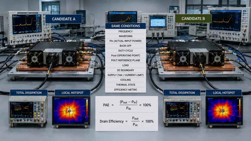
Do not mix these metrics. Also define whether driver stages, controls, auxiliary circuits, and fans are included in the DC boundary.
The operating point must match as well: frequency, waveform, duty cycle, Pout reference plane, Pin treatment, back-off, supply, thermal state, and cooling.
At the same operating point, higher efficiency generally means lower total electrical dissipation within the same boundary. It does not automatically mean a lower junction temperature or easier local cooling. Power density, package design, mounting, heat spreading, and thermal interfaces still determine how concentrated the heat becomes.
The buyer should therefore separate:
- total electrical dissipation;
- local thermal concentration;
- junction-temperature or interface risk;
- system cooling burden.
Condition-based RF PA heat-load estimation can quantify total dissipation, while RF PA thermal-management analysis addresses the cooling path. If the efficiency metric, reference plane, thermal state, or cooling boundary differs, mark the comparison Partially Comparable or Not Comparable Yet.
7. Do Linearity, Ruggedness, and Reliability Favor One Technology?
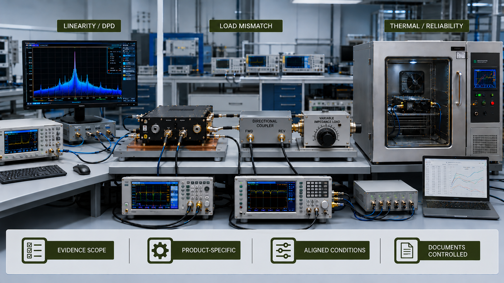
None of these attributes should be assigned to GaN or LDMOS without product-specific evidence.
Linearity and Back-Off
Linearity must use the same waveform, bandwidth, frequency, Pout reference plane, bias, back-off, and thermal state.
Digital predistortion (DPD) is signal processing used to reduce amplifier distortion. A result with DPD enabled is not directly equivalent to a result without DPD unless the comparison intentionally evaluates complete linearized systems.
If waveform, back-off, DPD condition, or thermal state differs, the candidates are Not Comparable Yet for linearity.
Load-Mismatch Ruggedness
A VSWR value alone does not establish ruggedness. The test boundary should define VSWR magnitude and phase, load reference plane, frequency, drive level, waveform, duration, thermal state, protection response, and recovery criterion.
Continued operation, power reduction, protective shutdown, survival without damage, and recovery are different outcomes. A larger isolated VSWR number is not automatically the better project result.
Reliability and Lifecycle Evidence
Reliability evidence must state whether it applies to a bare device, evaluation board, module, sample, batch, or fielded system. It should also identify stress conditions, duration, thermal state, failure criteria, and evidence scope.
Device-level evidence does not automatically prove module reliability, and one sample does not establish batch behavior. Implementation details such as mounting and thermal interfaces remain relevant to the result.
The buyer should request product-specific evidence for linearity, mismatch behavior, protection, and reliability under aligned conditions. If the methods or evidence scopes differ materially, hold the technology preference.
8. Compare Total System Cost and Supply Risk, Not Device Price
Device price is only one part of the route decision.

Acquisition Cost vs. Platform Cost
A useful comparison separates five effects: acquisition cost, integration cost, operating cost, redesign and requalification cost, and supply risk.
Platform cost can include the driver chain, power supply, bias system, matching, combining, control, linearization, cooling, enclosure, PCB area, and system power consumption. Changing technology may also require new validation, production-process changes, or recertification.
A lower-priced device can therefore lead to a higher-cost project, while a higher acquisition price does not guarantee lower total system cost either.
Supply Continuity and Requalification Risk
Neither GaN nor LDMOS is inherently safer from a supply-chain perspective. Review current lifecycle status, change-control policy, discontinuance notices, available alternatives, and the work required if a source changes.
An alternative device is not equivalent merely because it uses the same semiconductor technology. Electrical, thermal, mechanical, bias, matching, and qualification consequences may still require redesign.
Use current quotations and lifecycle evidence. Historical pricing or material-category assumptions are not enough to compare total route cost or continuity.
9. Build a Condition-Matched GaN vs. LDMOS Decision Matrix
Use the matrix to normalize evidence, not to create a universal score. Treat some conditions as hard gates and others as optimization items. If a hard gate remains Not Comparable Yet, do not hide the gap behind an overall score.
| Comparison Condition | Project Requirement or Hard Gate | GaN Candidate Evidence | LDMOS Candidate Evidence | Test Conditions and Reference Plane Aligned? | Comparability | Effect on Technology Route | Missing Evidence or Next Action |
|---|---|---|---|---|---|---|---|
| Frequency and instantaneous bandwidth | Required band, priority points, bandwidth | Product evidence across required range | Equivalent evidence across same range | Same frequency and bandwidth definition | Comparable / Partially Comparable / Not Comparable Yet | Validate the route that clears the hard gate with aligned evidence | Request missing band or frequency-point evidence |
| Pout definition and reference plane | Required Pout status and PA output plane | Product-specific Pout evidence | Equivalent evidence | Same definition, plane, waveform, and load | Comparable only when aligned | Remove candidates that miss a hard Pout gate | Clarify power status or obtain normalized data |
| Actual Pin and gain margin | Available Pin and required gain | Pin and gain evidence | Equivalent evidence | Same PA input reference plane and drive method | Comparable when aligned | Limited drive may change architecture priority | Request corrected Pin and gain data |
| Waveform, linearity, and back-off | Signal, duty cycle, peak-to-average ratio, linearity, back-off, DPD | Product evidence under stated conditions | Equivalent evidence | Same signal and processing conditions | Comparable only when equivalent | Keep only routes that satisfy the signal-quality gate | Request aligned testing |
| Efficiency metric and DC boundary | Selected metric and included DC loads | Condition-matched efficiency evidence | Equivalent evidence | Same Pout, Pin, supply, waveform, thermal state | Comparable when aligned | Lower verified dissipation may improve system fit | Normalize metric or request new data |
| Total and local thermal burden | Total heat, local heat concentration, hot-state requirement | Stabilized thermal evidence | Equivalent evidence | Same ambient, mounting, cooling, duration | Comparable when aligned | Thermal bottlenecks can change route priority | Request stabilized thermal evidence |
| Cooling and enclosure | Cooling capacity and enclosure limits | Integration requirements | Equivalent requirements | Same installation boundary | Comparable when aligned | Reject routes that cannot meet sustained cooling limits | Complete cooling review |
| SWaP and mechanical envelope | Size, weight, power, interfaces | Current mechanical and power data | Equivalent data | Same integration level | Comparable when aligned | Tight SWaP can change route priority | Request drawings and interface details |
| Load mismatch and protection | VSWR, phase, duration, protection, recovery | Product-specific mismatch evidence | Equivalent evidence | Same load plane and test conditions | Not Comparable Yet if methods differ | Follow the route that meets the required mismatch outcome | Request aligned tests |
| Platform reuse | Reusable electrical, thermal, mechanical, production assets | GaN-route change scope | LDMOS-route change scope | Same baseline platform | Partially Comparable until scope is defined | Reuse can materially change total project risk | Build a controlled change list |
| Redesign and requalification | Engineering, testing, production, certification work | Route-specific estimate | Equivalent estimate | Same project scope | Comparable only when scope matches | Requalification burden may reverse an acquisition advantage | Complete engineering estimate |
| Lifecycle and supply continuity | Required service life and change-control expectations | Current lifecycle evidence | Equivalent evidence | Same date and product scope | Not Comparable Yet when evidence is incomplete | Continuity evidence may retain or remove either route | Request current lifecycle and change-control evidence |
The matrix should end in one of the four routes defined earlier. If a decisive row is still Not Comparable Yet, the correct result is to pause rather than rank the technologies.
Turn the Technology Decision Into an RFQ Evidence Request
The RFQ should normally stay technology neutral unless certification, compatibility, or supply requirements make the semiconductor material a hard constraint.
Only candidates that are sufficiently comparable in the decision matrix should enter the technical shortlist. Unresolved hard gates remain supplier evidence requests.
| RFQ Requirement | Project Condition or Permitted Range | Evidence the Supplier Should Submit | Operating or Test Conditions Required for the Evidence | Applicable Product, Configuration, or Sample Scope | Use: Qualification, Candidate Comparison, or Later Verification | Action if Unmet |
|---|---|---|---|---|---|---|
| ☐ Working frequency and instantaneous bandwidth | Required range, priority points, bandwidth | Current product data or report | Required frequencies and operating state | Named product or configuration | Qualification and comparison | Request missing range evidence |
| ☐ Target Pout and reference plane | Pout status and PA output plane | Product-specific specification or test data | Frequency, waveform, Pin, load, thermal state | Named product and sample scope | Qualification and verification | Hold qualification until aligned evidence is supplied |
| ☐ Available actual Pin and gain | Available Pin and required margin | Pin and gain evidence | Defined PA input plane and drive method | Proposed signal chain | Qualification and comparison | Clarify drive boundary or revise architecture |
| ☐ Waveform, linearity, back-off, and DPD | Signal, duty cycle, peak-to-average ratio, linearity, back-off, DPD state | Condition-matched output and linearity evidence | Same waveform, bandwidth, back-off, and thermal state | Named module and processing configuration | Qualification and verification | Request aligned testing |
| ☐ Supply and efficiency boundary | Supply limits, metric, included DC loads | DC input, RF output, efficiency data | Same Pout, Pin treatment, waveform, and hot state | Complete module or subsystem boundary | Comparison and qualification | Normalize the boundary or request new evidence |
| ☐ Thermal and cooling conditions | Ambient, baseplate or case temperature, cooling, duration | Thermal operating evidence | Required Pout, mounting, cooling, and stabilized state | Proposed mounted configuration | Qualification and verification | Hold sustained-operation decision |
| ☐ Size, weight, interfaces, and platform limits | Mechanical and interface constraints | Drawing, mass, interfaces, change list | Proposed production configuration | Named module or subsystem | Qualification and comparison | Reject or revise if a hard limit is missed |
| ☐ Load, VSWR, protection, and recovery | Load plane, VSWR, phase, duration, allowed response | Product-specific mismatch evidence | Required drive, waveform, temperature, and duration | Named product and protection configuration | Qualification and verification | Keep the item open until aligned evidence exists |
| ☐ Permitted amplifier architecture | GaN, LDMOS, hybrid, dual-candidate, or technology-neutral | Architecture disclosure | Complete proposed signal chain | Full proposed configuration | Qualification and comparison | Clarify unexplained material restrictions |
| ☐ Document version and evidence scope | Required revision and evidence level | Controlled documents with date and scope | Conditions must match the project or state limitations | Named product, configuration, and sample scope | Qualification and verification | Request the correct evidence scope |
| ☐ Lifecycle and source changes | Required lifecycle, change notification, alternatives, requalification | Current lifecycle and change-control evidence | Current date and explicit product scope | Named device and module configuration | Supplier qualification | Keep continuity assessment open |
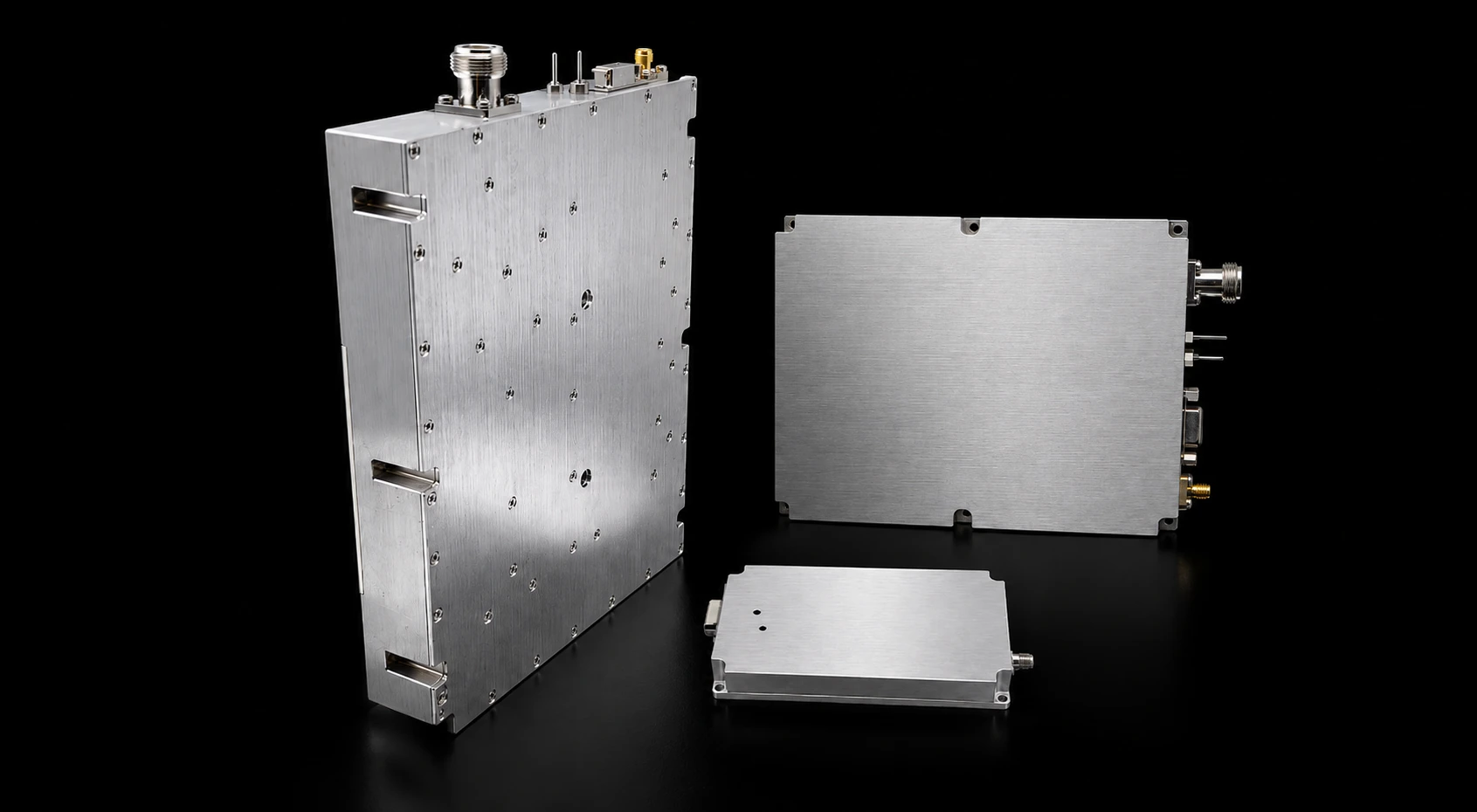
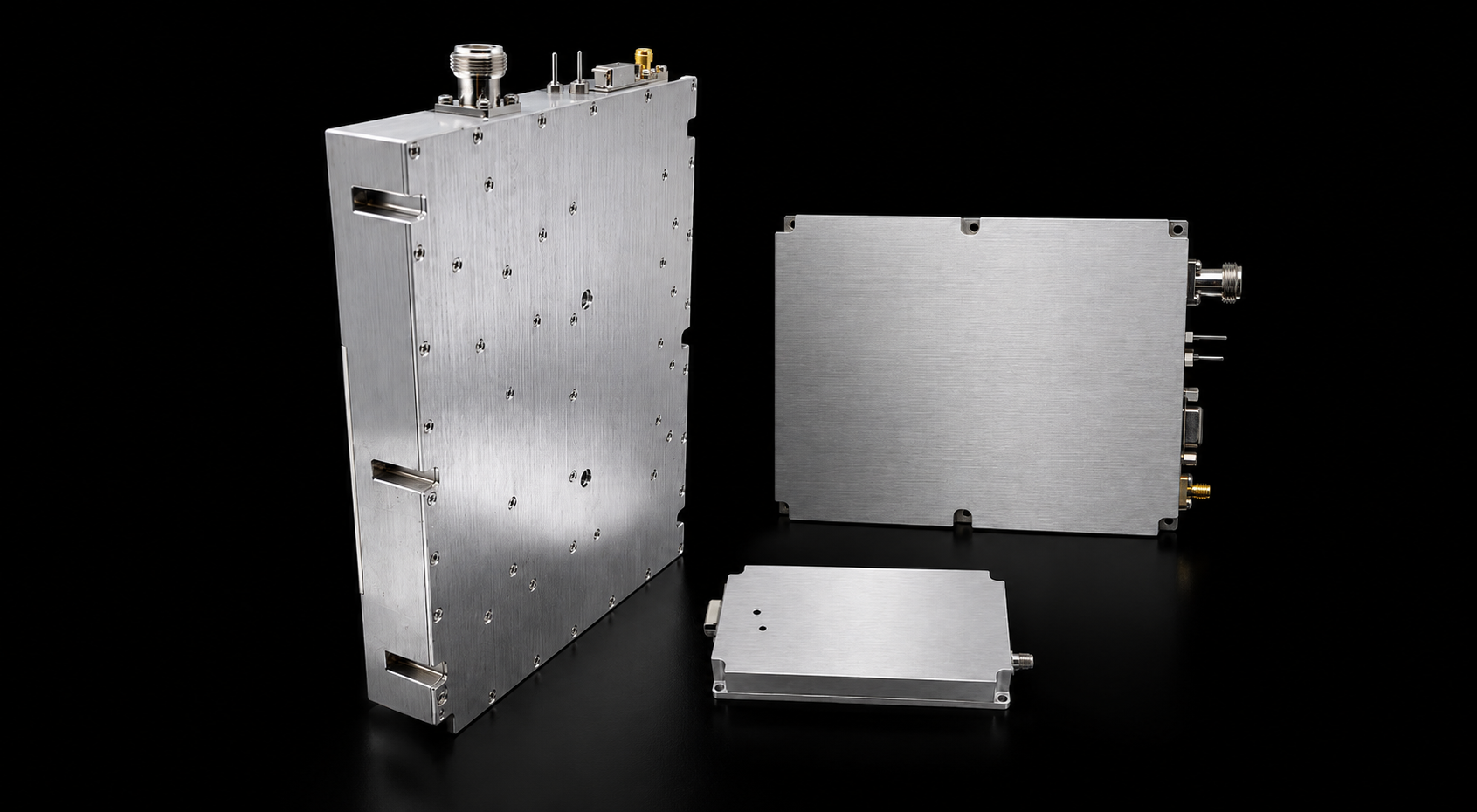
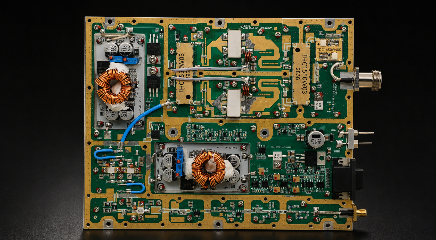
Once these inputs are defined, standard and custom RF PA modules can be used as a candidate-discovery starting point. Projects with genuine continuous wideband, multiband, or wide instantaneous-bandwidth requirements can also review the wideband RF PA product range. Product categories do not by themselves prove semiconductor technology or project suitability.
Where public product categories do not map the requirement, the completed application boundary and evidence checklist can be submitted for RF PA engineering review.
Choose the Next RF PA Review Route
Conclusion
GaN and LDMOS have no application-independent winner. Prioritize GaN when higher-frequency operation, wide bandwidth, power density, gain, or SWaP constraints make it the stronger validation route. Prioritize LDMOS when the same hard requirements are met and qualified-platform reuse or total project cost makes it the lower-risk route. Keep a hybrid or dual-candidate path when more than one architecture remains viable, and pause whenever a decisive condition is still Not Comparable Yet.
That conclusion is valid only when frequency, bandwidth, Pout and its reference plane, Pin, waveform, back-off, efficiency boundary, thermal state, cooling, load, platform scope, and evidence range are defined. This framework can identify a technology-validation route and the evidence a supplier must provide; it cannot approve a specific model, prove the technology used in a particular RF SKYPOWER product, or replace project testing and final acceptance.
The next independent action is to complete the application boundary, finish the decision matrix, resolve every hard evidence gap, and convert the selected route into the RFQ checklist.
After that, use the standard and custom RF PA module range or, where wide bandwidth is a real project constraint, the wideband RF PA module range for candidate discovery. Then submit the complete application and evidence requirements to RF SKYPOWER for product-range or project engineering review. The review request does not confirm a specific technology, model, performance result, price, availability, delivery, or acceptance outcome.