How Transistor Attach Affects RF PA Thermal Performance
August 3, 2026
Two RF PA modules can use the same GaN transistor, the same PCB layout, the same copper structure, and the same external heatsink—yet begin to separate after heat builds.
One module may hold its output and gain. Another may draw more current, run hotter, lose margin at a critical frequency, or reach temperature protection sooner.
That difference in RF PA thermal performance creates a difficult approval question:
If the GaN device is the same, what changed inside the finished module?
The obvious answer is to suspect the transistor itself. But the device part number controls only one part of the completed RF PA.
Bias, matching, grounding, actual RF drive, generated heat, load conditions, and external cooling can all change hot-state behavior. There is also another variable that customers rarely see after assembly: the way the final-stage RF power transistor becomes connected to the copper structure and surrounding RF circuit.
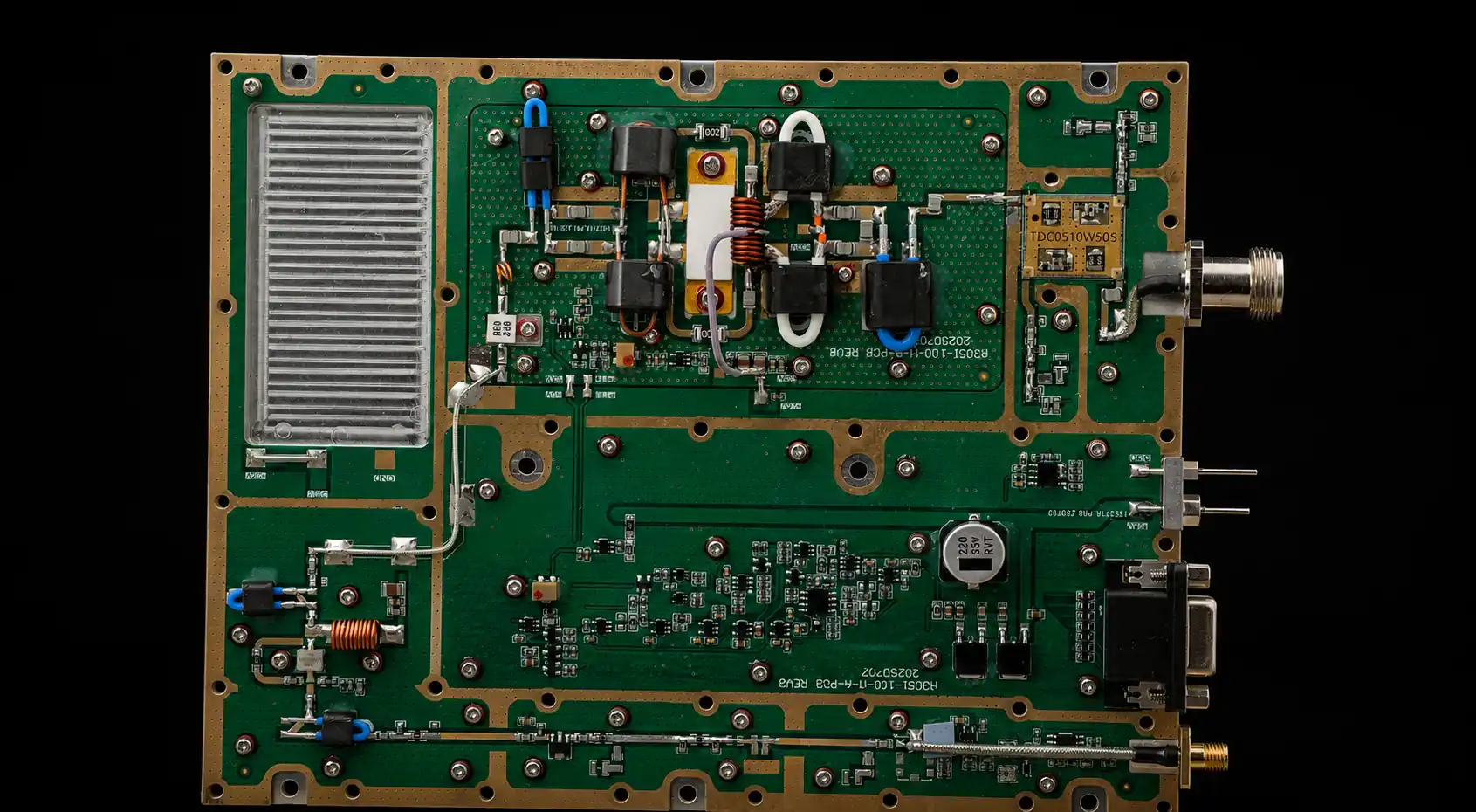
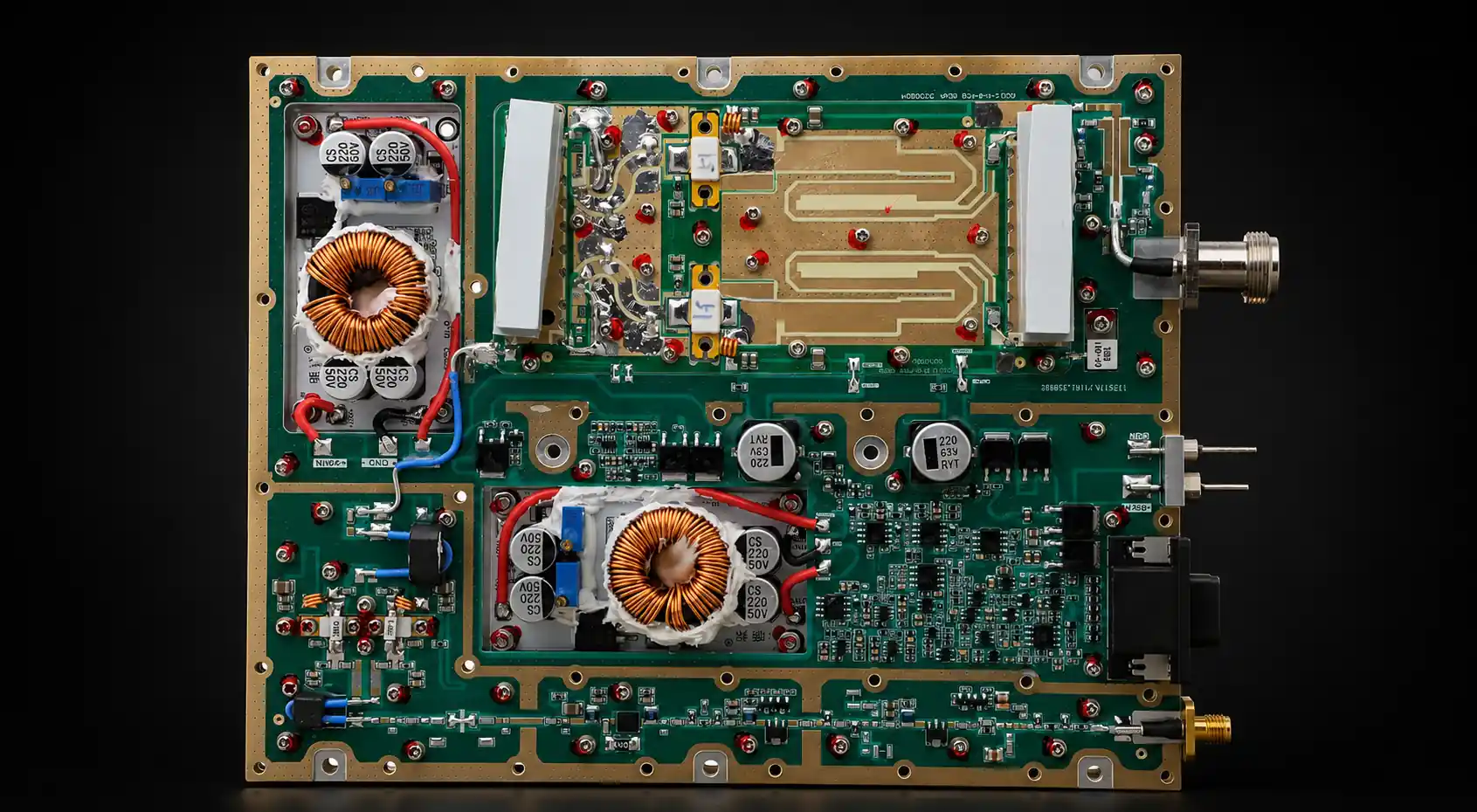
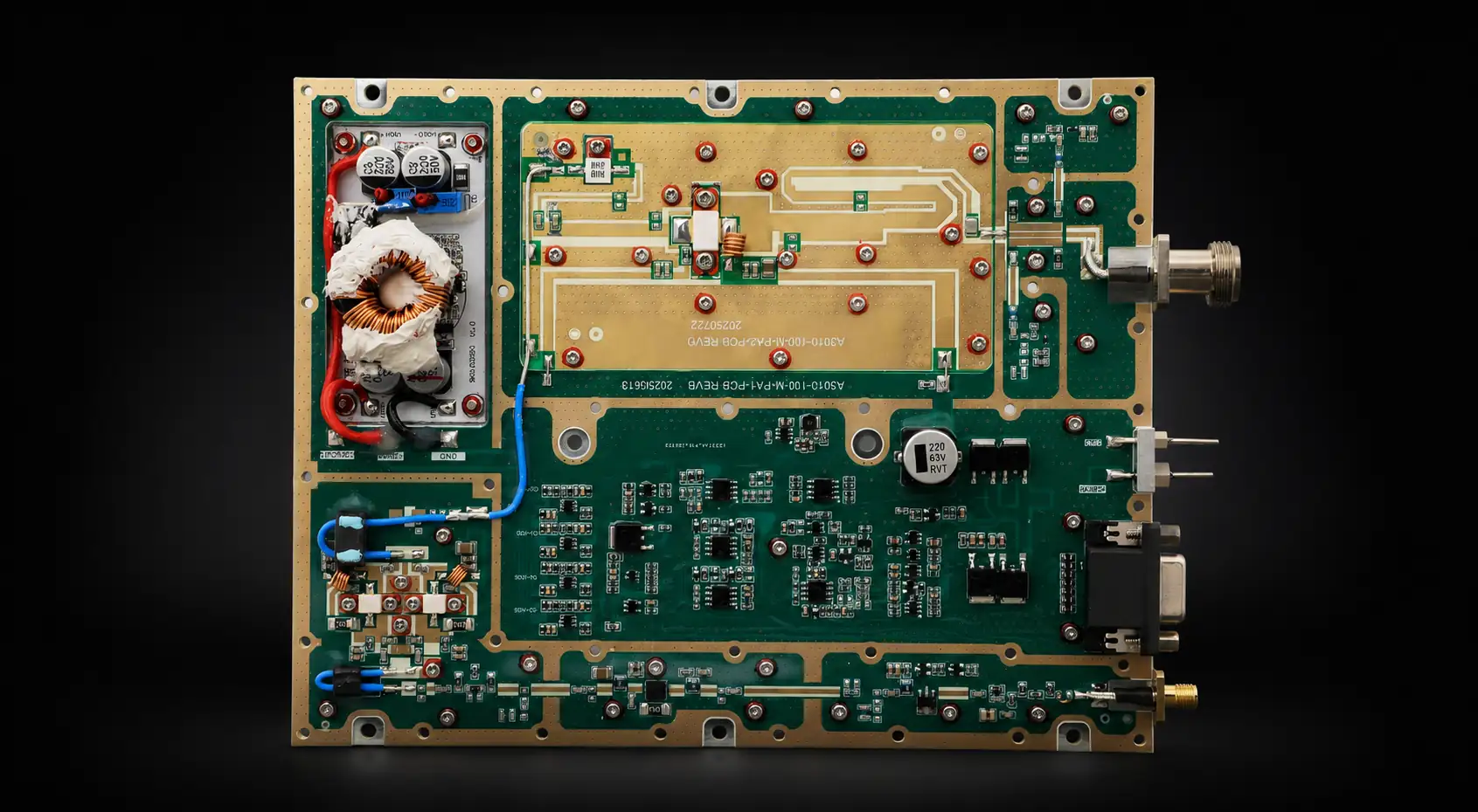
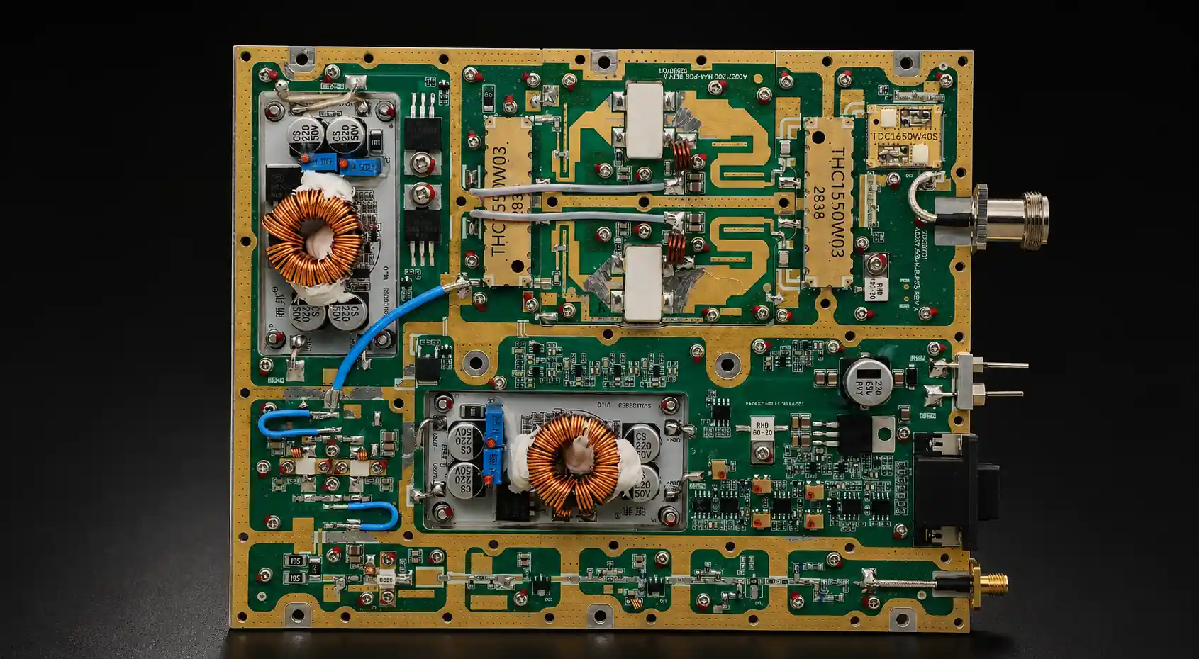
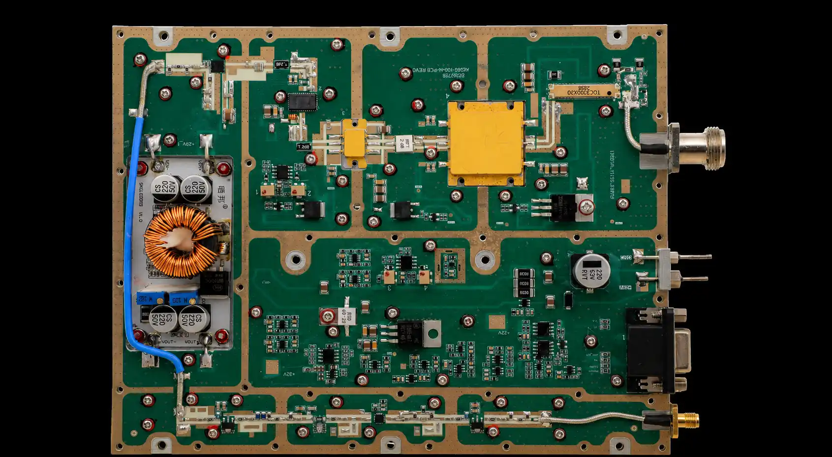
Depending on the package architecture, the transistor’s thermal base may attach to a copper carrier or module base, while its RF leads connect to the surrounding PCBA. Once installed, these thermal, electrical, and mechanical connections become hidden inside the finished module.
At RF SKYPOWER, this attachment stage integrates the packaged final-stage transistor into the RF assembly after the PCBA has been secured within the copper structure.
The process is easy to overlook because the completed interface disappears beneath the transistor package. Yet after power is applied, that hidden connection becomes part of the path carrying heat away from the device and connecting it to the RF matching, grounding, and mechanical structure.
The next question is not whether the attachment exists. It is whether the completed module still maintains acceptable current, gain, output, temperature, and protection behavior after the entire assembly reaches its defined hot-state condition.
1. Why the GaN Part Number Does Not Define the Full Module
A GaN transistor part number identifies the active device and its package. It does not define the complete thermal, electrical, and mechanical structure of the finished RF PA.
For a device package with a dedicated thermal base or flange, the main heat path may be represented as:
Semiconductor junction → Package thermal base or flange → Attachment interface → Copper carrier or module base → External thermal interface → Heatsink or cold plate
The RF signal connection may follow a different path:
Package RF leads → Solder joints → Matching network on the RF PCBA
The exact paths depend on the package and module design. The RF PCBA should not automatically be treated as part of the main vertical heat-transfer path.
A device datasheet may specify junction-to-case thermal resistance under defined test conditions. That value does not define:
package-to-base attachment resistance;
base-to-housing thermal resistance;
external thermal-interface resistance;
heatsink-to-ambient performance;
airflow or cold-plate capacity;
production variation in the completed assembly.
The finished module also depends on bias, matching, grounding, actual Pin, supply voltage, output loading, protection settings, and cooling.
Two modules using the same GaN transistor may therefore behave differently after heat builds.
One module may require more current to produce the same output. Another may lose more gain at a project-critical frequency. A third may approach its protection boundary sooner.
These differences do not prove that the transistor attachment is responsible. They show why device identity alone is not enough to approve the finished RF PA.
The GaN part number identifies the active device, but it does not define the complete operating behavior of the finished module.
2. Where the Hidden Attach Interface Sits in the RF PA
The final-stage component is a packaged RF power transistor rather than a bare semiconductor die.
Its thermal base, RF leads, and grounding connections may follow different physical paths within the assembly.
During production, the transistor package is positioned within the RF structure and connected through a defined attachment process. Depending on the design:
the thermal base or flange may attach to a copper carrier or module base;
the RF leads may connect to the surrounding matching network;
grounding may depend on the flange, source leads, or another defined connection;
package position may affect lead alignment and RF geometry.
These connections become part of the module’s operating structure.
The attachment beneath the thermal base influences how heat moves away from the transistor package. The RF lead connections affect how the device interacts with the matching network. Grounding and positioning can affect current flow, stability, and production repeatability.
Once the transistor has been installed, the internal interface cannot normally be judged from the device part number or the external appearance of the finished module.
This is why transistor attachment remains important even when the incoming GaN device is genuine, correctly identified, and electrically qualified.
Variation at this stage does not automatically create a field failure. It does, however, become one of the hidden production variables that must remain controlled when multiple modules are expected to show comparable hot-state behavior.
The transistor-attach interface is where the packaged device becomes part of the module’s heat path, RF path, grounding structure, and mechanical assembly.
3. What Hot-State Differences Can—and Cannot—Tell You
Temperature is a visible symptom. It is not a standalone diagnosis.
A higher case or copper-base temperature does not automatically mean that the transistor attachment has higher thermal resistance.
A lower external temperature does not automatically mean that the attachment is better.
If an attachment interface restricts heat transfer, the semiconductor junction may become hotter while a downstream base sensor rises more slowly. Conversely, a warmer copper base may indicate that heat is transferring into the base effectively but is not being removed efficiently by the external heatsink.
Case, base, housing, and heatsink temperatures are also not interchangeable with junction temperature. Each measurement location represents a different point in the thermal path and may respond with a different delay.
A meaningful comparison should use the same:
sensor type and attachment method;
measurement location;
ambient condition;
sampling interval;
stabilization rule.
Generated Heat Must Be Compared First
Two RF PA modules producing the same output power may not generate the same internal heat.
The relevant DC input power is:
Total DC Input Power = Σ(Vdc × Idc)
Estimated internal dissipation may be expressed as:
Estimated Dissipated Power ≈ Total DC Input Power + RF Input Power − Total Delivered RF Output Power
All power terms must be converted to linear watts and linked to defined reference planes. Values expressed in dBm must not be added or subtracted directly.
Where multiple DC rails are used, the relevant input powers should be summed. Where only corrected fundamental Pout is available, the dissipation result should be identified as an estimate because harmonic and other RF output components may not be included.
Consider two modules that both reach the required Pout:
Module A reaches the target with lower Idc.
Module B reaches the same target but draws more current.
If Module B runs hotter, the difference may come from lower efficiency and greater internal heat generation rather than from a poorer transistor attachment.
Hot-state variation may justify further investigation, but it cannot identify one hidden interface as the root cause until RF, DC, load, cooling, and measurement conditions are controlled.
The correct question is not simply which module is hotter. It is which module runs hotter under comparable dissipated power, RF output, cooling, and measurement conditions.
4. Why a Short Cold Test May Miss the Difference
A short cold-state test can confirm that the RF PA initially operates.
It may show that:
the module powers on;
basic gain is present;
output reaches the target;
no immediate protection event occurs.
That information is useful, but it may not reveal differences that appear only after the transistor package, copper structure, housing, and cooling system approach a comparable thermal state.
As heat builds, a module may show:
changing Idc;
reduced large-signal gain;
falling Pout margin;
greater variation at project-critical frequencies;
a different external temperature trend;
earlier protection foldback;
slower recovery after RF drive is removed.
A valid hot-state comparison should keep the main operating boundaries consistent:
frequency and actual Pin;
corrected Pout;
Vdc and Idc;
estimated dissipated power or efficiency;
load and duty conditions;
cooling and ambient conditions;
temperature-measurement location;
protection configuration.
Thermal Stability Must Be Defined
A fixed operating time does not automatically mean that every module has reached a comparable thermal state.
The test plan may define stabilization through:
a validated dwell time;
a maximum temperature-change rate over a defined interval;
a combination of time and temperature criteria.
The same rule should be applied to every compared module.
A 100 W, 150 W, or 200 W RF PA does not have one universal stabilization time. The required duration depends on efficiency, duty condition, mechanical construction, cooling capacity, ambient temperature, and sensor location.
A controlled full-power RF PA test should therefore connect output, current, temperature, load, cooling, duration, and protection status rather than recording only a brief cold-state result.
A cold-state PASS confirms initial operation. It does not prove that current, gain, output, temperature, and protection behavior will remain consistent after heat builds.
5. What Evidence Supports Repeatable Production
The hidden attachment cannot be evaluated through one record alone.
A practical review combines three evidence layers:
Process control → How the attachment conditions were kept repeatable
Inspection evidence → What was checked after assembly
Hot-state RF evidence → How the finished module performed
Process Control
The supplier should control:
approved attachment material and handling;
surface preparation and package positioning;
heating recipe and equipment;
inspection method;
process revision and rework traceability.
The customer does not need the complete proprietary process recipe. It does need confidence that approved materials and production conditions are documented and that changes cannot enter production informally. For the manufacturing-side approval boundary, the RF power transistor soldering review connects the attach process with applicable inspection, finished-module RF evidence, and S/N-linked traceability.
Changes to materials, fixtures, equipment, process settings, or rework methods should follow documented RF PA process-change control and be linked to the affected configuration or S/N range.
Inspection Evidence
The inspection method should match the actual package construction and factory quality plan.
Depending on the approved process, inspection may include:
visual alignment checks;
X-ray inspection;
defined coverage or void criteria;
bond-line assessment;
process qualification;
destructive cross-section sampling for qualification or failure analysis.
Visual inspection can identify obvious positioning problems. It cannot determine the complete internal interface condition.
X-ray capability depends on package construction, metal thickness, imaging geometry, and equipment resolution. Destructive cross-section work is normally used for process qualification or failure analysis rather than as a shipment inspection for every module.
Hot-State RF Evidence
Process control shows how the attachment conditions were managed. Finished-module evidence shows whether the complete assembly operated inside its approved boundaries.
A hot-state production record may include:
module model and S/N;
hardware and process revision;
frequency and actual Pin;
corrected Pout and large-signal gain;
Vdc and Idc;
efficiency or estimated dissipated power;
measured temperature and sensor location;
stabilization rule;
load and cooling conditions;
protection status;
acceptance limits and result.
Every delivered module should have an S/N-linked production report. The depth of hot-state testing may follow the approved acceptance plan, but the data must belong to the delivered unit.
A controlled S/N-linked RF PA test report allows the buyer to confirm which module was tested, under which operating boundaries, and why it was released.
What Each Evidence Layer Supports
Evidence
What it supports
What it cannot establish alone
Device identity record
Correct transistor part number and controlled substitution
Completed-module thermal consistency
Attach-process record
Approved materials and production conditions were used
Internal interface condition of every unit
Inspection record
Defined attachment characteristics were checked
Hot-state RF performance
Cold-state RF test
Initial operation, gain, and output
Thermally stabilized behavior
Hot-state S/N report
Finished-module performance under defined conditions
Transistor attachment as the sole root cause
Batch comparison
Production spread under one test boundary
Long-term field reliability by itself
Process control supports repeatability at the manufacturing stage; hot-state RF evidence confirms whether the completed module meets its operating requirements.
6. What Buyers Should Ask Before Approval
The buyer does not need every proprietary detail of the attachment process.
It does need enough evidence to determine whether the approved construction is controlled and whether production modules are compared under meaningful hot-state conditions.
RFQ Checklist
RFQ item
What to ask or define
What it confirms
Device and architecture
Final-stage part number, package type, substitution rule, and connection architecture
The active device and main thermal/RF paths are controlled
Attach process
Approved material, surface preparation, positioning, heating process, and revision
Attachment conditions are repeatable
Inspection method
Visual, X-ray, qualification, or another method actually used
The completed attachment receives a defined check
Rework and change control
Authorization, records, affected S/N range, and required reverification
Adjusted units and process changes remain traceable
Hot-state boundary
Frequency, Pin, Pout, duty, load, cooling, and stabilization rule
Modules are compared under equivalent conditions
Thermal test record
Vdc, Idc, efficiency or dissipation, sensor location, ambient condition, and temperature
Temperature is interpreted against generated heat and a defined measurement boundary
Protection evidence
Protection revision, threshold, and operating status
Protection timing is reviewed in the correct configuration
S/N-linked release report
Unit results, limits, margin, exceptions, and release status
Evidence belongs to the delivered module
Supplier batch review
Multiple production S/N units reviewed under one approved boundary
Production spread is monitored before shipment
If one production module shows different temperature, current, gain, output, or protection behavior, the supplier should first confirm that it was compared under equivalent RF, DC, dissipated-power, load, cooling, and measurement conditions.
Only after those variables have been checked should the transistor-attach interface become a root-cause candidate.
The buyer does not need the supplier’s complete process recipe. It needs enough process control and hot-state evidence to confirm that the approved module construction can be repeated in production.
Conclusion
The same GaN transistor does not guarantee identical RF PA temperature, current, gain, output margin, or protection behavior.
The final-stage transistor becomes part of the completed module through interacting thermal, electrical, and mechanical connections. Its attachment is therefore an important production variable—but it must be evaluated together with generated heat, bias, matching, load, cooling, and measurement conditions.
RF SKYPOWER can support early engineering review of the transistor package, attachment architecture, operating frequency, output target, cooling boundary, hot-state test conditions, protection behavior, and S/N-linked evidence before final module approval.
Contents
About Our Company
RF SKYPOWER is a Source Factory engineering precision RF modules, antennas, SDR signal sources, and detection systems built exclusively for defense, security, and critical infrastructure applications.
When R&D, manufacturing, and testing happen under one roof, you get unmatched quality control and supply chain stability.