
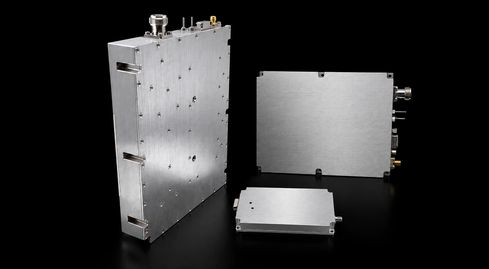
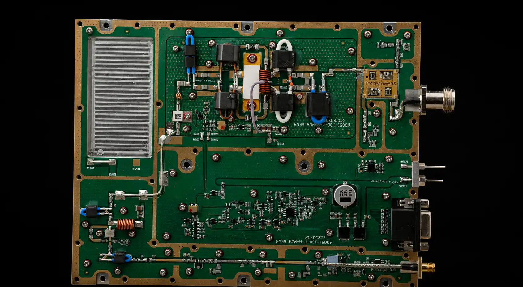
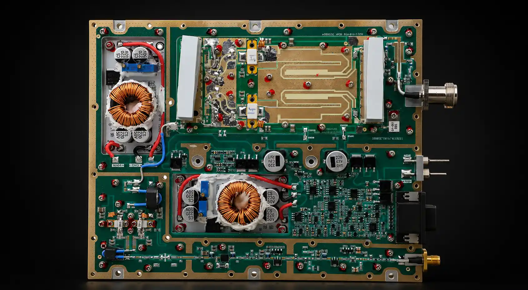
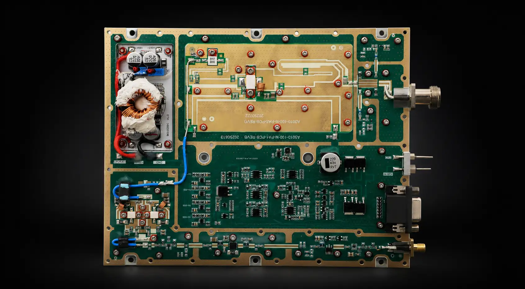
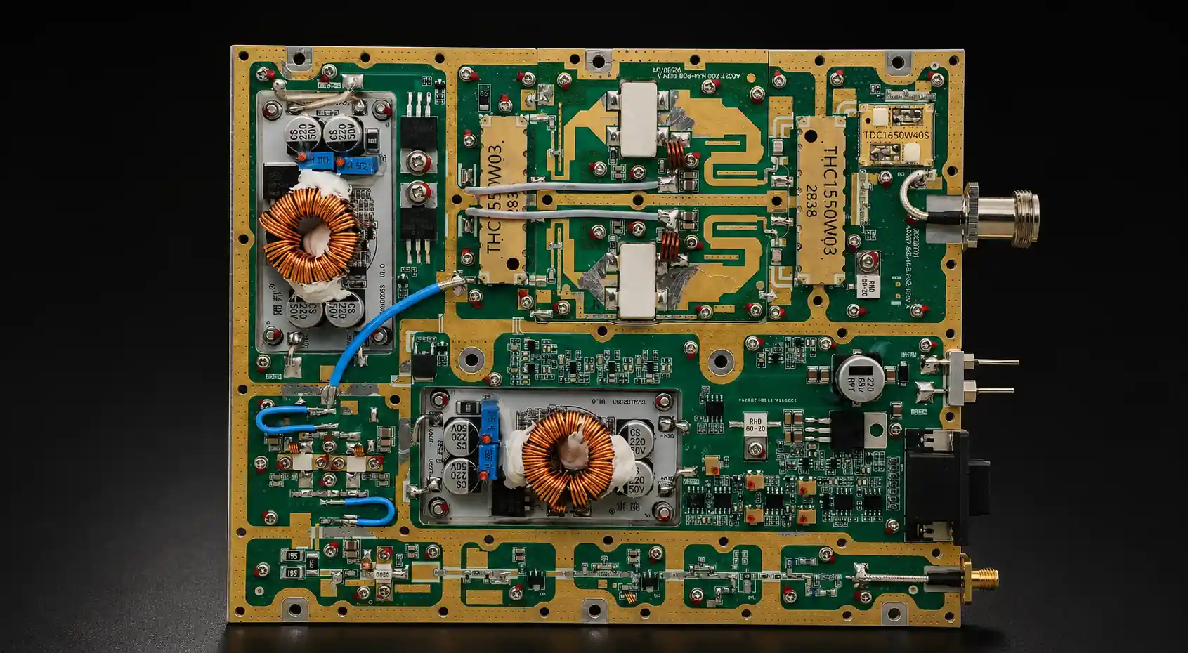
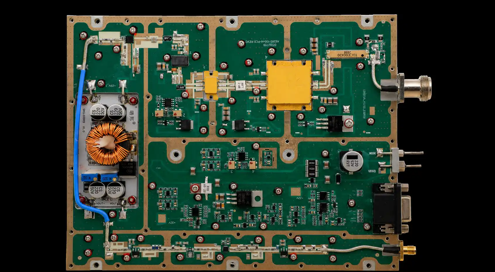


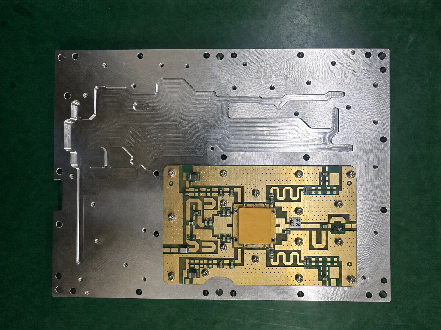
RF power transistor soldering is mostly hidden after the final-stage device is installed. A factory video may show a clean reflow process, and the finished PA may still reach its required output during an initial test. Neither result alone tells the buyer whether the hidden attachment interface is controlled well enough for production approval.
The difficulty is that a later hot-state difference does not automatically prove a solder-attach defect either. Bias, actual RF drive, generated heat, load, cooling, matching, and protection behavior can produce similar symptoms.
That leaves a more useful procurement question:
What manufacturing, inspection, and finished-module evidence should be connected before RF power transistor soldering is accepted as a controlled production process?
1. Why a Qualified RF Power Transistor Does Not Prove the Solder Attach
A qualified RF power transistor and a qualified transistor-attach process answer different questions.
Device-level evidence may identify or verify items such as:
- Approved transistor type
- Manufacturer and part number
- Device lot or traceability information
- Incoming inspection status
- Electrical screening where applicable
That evidence is important, but it does not prove how the device was attached to the RF PA structure.
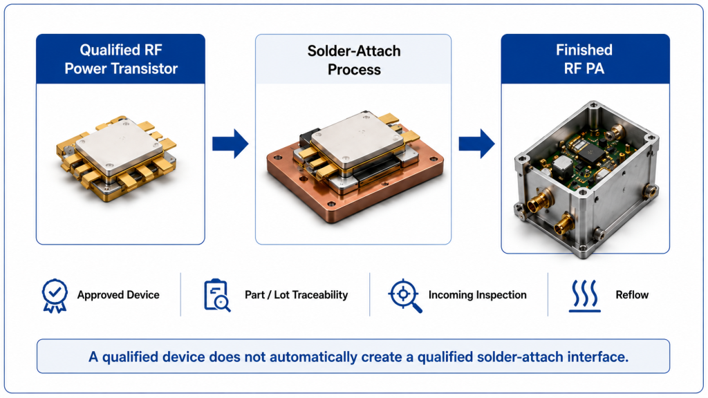
Once the transistor enters assembly, additional manufacturing variables become relevant:
- Solder application
- Device positioning
- Contact between the transistor package and attachment surface
- Reflow condition
- Cooling after reflow
- Joint condition
- Process repeatability
- Hidden-interface inspection where applicable
A qualified semiconductor can therefore enter a poorly controlled assembly process, while a controlled assembly process cannot compensate for an incorrect or defective semiconductor.
For PA approval, the buyer should keep these evidence layers separate:
Device identity → Attachment process → Inspection evidence → Finished-module test evidence
Passing one layer does not automatically prove the next. For GaN-based designs, the separate GaN device quality review covers device identity, lot control, incoming evidence, and the boundary between semiconductor approval and finished-module approval.
2. How Is the RF Power Transistor Solder Attach Process Controlled?
The final-stage transistor attachment may be described as RF Power Transistor Solder Attach or Final-Stage RF Power Transistor Reflow Soldering, depending on the package and manufacturing documentation.
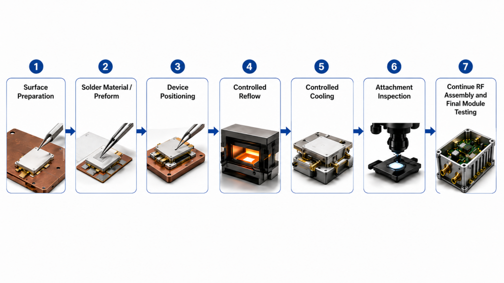
A simplified manufacturing sequence may include:
- Preparing the attachment surface
- Applying the defined solder material or solder preform
- Positioning the RF power transistor
- Running the required reflow process
- Allowing the assembly to cool under the defined process
- Inspecting the finished attachment
- Continuing RF assembly and final module testing
The exact process depends on the transistor package, module structure, solder system, and approved production method.
What Should the Process Record Preserve?
Depending on the approved manufacturing process, relevant records may include:
- Transistor identity
- Assembly lot or work order
- Solder material or preform identification
- Process specification or approved work instruction
- Reflow profile or controlled process condition
- Operator or station traceability
- Inspection result
- Rework status where applicable
The objective is not to create paperwork for its own sake. The objective is to make the attachment process reproducible and auditable when a later RF or thermal result needs to be investigated.
3. Where Does the Attach Interface Sit in the RF PA?
The transistor attachment interface can affect mechanical support, electrical behavior, grounding, and heat transfer, but its exact role depends on the transistor package and RF PA architecture.
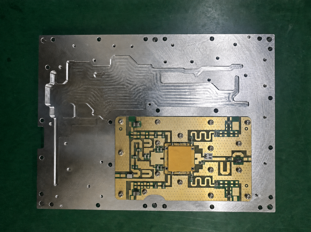
For a package with a dedicated thermal base or flange, a simplified main heat path may be represented as:
Semiconductor junction
→ Package thermal base or flange
→ Attachment interface
→ Copper carrier or module base
→ External thermal interface
→ Heatsink or cold plate
The RF leads may follow a different connection path:
Package RF leads
→ Solder joints
→ Matching network on the RF PCBA
These paths should not be treated as identical.
A transistor with a dedicated thermal base should not automatically be described as dissipating its main heat through the RF PCB merely because its RF leads are soldered to that PCB.
The exact thermal, RF, and grounding paths depend on:
- Package architecture
- Attachment surface
- Copper carrier or module-base design
- Matching-network layout
- Ground structure
- External heatsink or cold-plate interface
This distinction matters when a finished module later shows abnormal hot-state behavior.
A problem at the transistor attachment interface is only one possible contributor. A separate module-base-to-heatsink thermal interface, such as thermal grease or another interface material, belongs to a different physical boundary and should be evaluated separately.
4. What Hot-State Symptoms Can—and Cannot Prove About Solder Attach
An attachment problem may become more visible after heat builds, but a hot-state symptom is not the same as a confirmed solder-attach root cause.
Possible symptoms may include:
- Faster-than-expected temperature rise
- Hot-state gain change
- Pout change after thermal stabilization
- Idc change
- Earlier compression
- Protection activation
- Unit-to-unit thermal differences
These observations can justify investigating the transistor-attach interface.
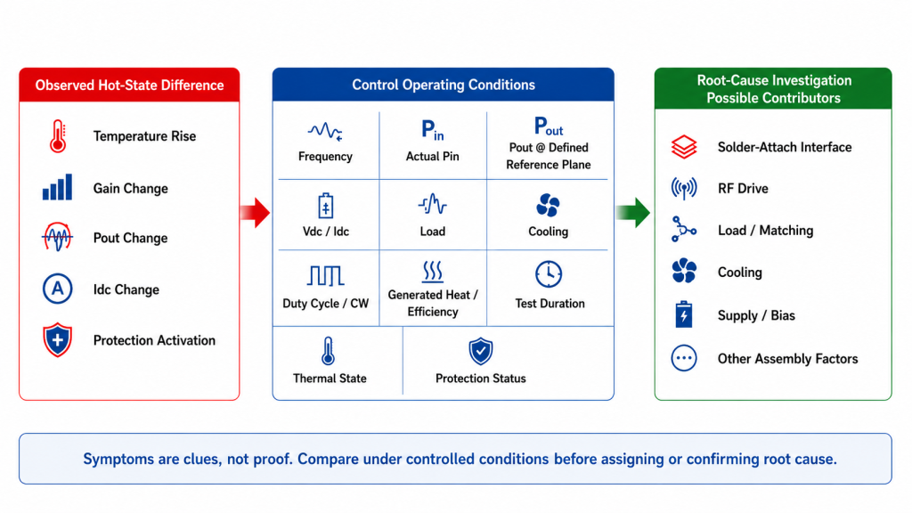
They do not prove that the interface is defective.
Before assigning root cause, engineers should compare the relevant operating conditions, including:
- Frequency
- Actual Pin at the PA input
- Pout at a defined reference plane
- Vdc
- Idc
- Load condition
- Duty cycle or CW condition
- Cooling condition
- Test duration
- Thermal state
- Protection status
Generated heat also matters.
Two modules should not be compared only by surface temperature if one is operating at a different RF output, DC input, efficiency, waveform condition, or cooling boundary.
A hotter unit may have an attachment problem, but it may also be dissipating more heat for another reason.
The technically safe conclusion is:
A hot-state difference can make the transistor-attach interface a root-cause candidate, but it cannot identify that interface as the cause until RF drive, generated heat, load, cooling, supply, measurement conditions, and protection state are controlled.
This distinction protects the approval process from diagnosing the wrong manufacturing problem. For the deeper thermal and root-cause boundary, see how transistor attach affects RF PA thermal performance under controlled RF, DC, load, cooling, and measurement conditions.
5. How to Build the Evidence Chain for Solder-Attach Approval
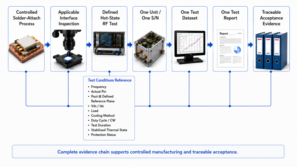
Solder-attach approval should not depend on one type of evidence. A stronger decision connects manufacturing process control, applicable interface inspection, finished-module hot-state behavior, and unit-level traceability.
Process evidence shows how the attachment stage was controlled.
Inspection evidence shows what characteristics of the assembled interface were checked.
Finished-module RF evidence shows how the completed RF PA behaved under the defined operating condition.
S/N-linked traceability connects that finished result to the delivered unit.
None of these evidence layers alone proves the entire manufacturing chain.
Define the Finished-Module Test Condition
A useful finished-module hot-state record should identify the conditions that materially affect the conclusion, such as:
- Frequency
- Actual Pin
- Pout
- Output measurement reference plane
- Vdc
- Idc
- Load
- Duty cycle or CW condition
- Cooling method
- Test duration
- Stabilized thermal state
- Protection or alarm status
If the measurement path includes cables, attenuators, couplers, connectors, or other RF components, the report should also state the relevant correction and reference plane.
A cold-state pass should not automatically be treated as a stabilized hot-state pass.
Likewise, a hot-state failure should not automatically be labeled a solder-joint failure.
For the complete PA-side test methodology, the finished module can be evaluated using a defined full-power RF PA test under controlled frequency, input-drive, load, cooling, and thermal conditions.
Hidden-Interface Inspection
Because the attach interface may no longer be directly visible after assembly, inspection may require evidence beyond external appearance.
Depending on the package and approved manufacturing process, this may include:
- Visual inspection of accessible joint areas
- Process records
- Controlled reflow data
- Dimensional or mechanical inspection
- X-ray or another hidden-interface inspection method where applicable
- Destructive analysis for qualification or failure investigation where justified
No single inspection method should be presented as universally required for every transistor package.
The inspection method should match the package structure, manufacturing risk, qualification plan, and acceptance requirement.
Connect the Finished Result to the Delivered Unit
When unit-level shipment evidence is required, the finished-module result should remain linked to the delivered serial number rather than stored as a generic batch screenshot.
A stronger acceptance chain is:
One Unit
→ One Serial Number
→ One Test Dataset
→ One Test Report
→ Traceable Acceptance Evidence
This is where manufacturing control becomes commercially useful.
A buyer does not only need to know that a production process exists. The buyer may also need evidence showing which finished RF PA was tested, under what conditions, and which report belongs to that delivered unit. For the broader shipment-release boundary, the C-UAS RF PA acceptance checklist separates per-unit, batch-level, configuration-level, and project-level evidence.
6. What Evidence Should Buyers Require Before Solder-Attach Approval?
The RFQ or approval process should separate four evidence types:
| Evidence Area | Buyer Should Ask | What It Can Prove | What It Cannot Prove Alone |
|---|---|---|---|
| Device identity | What transistor type, approved source, and traceability apply? | The intended device entered production | That the device was attached correctly |
| Manufacturing process | What solder-attach process and controlled work instruction are used? | The attachment stage is defined and controlled | The internal condition of every finished joint |
| Inspection | What inspection method applies to the hidden interface? | The specified interface characteristics were checked | Finished RF performance under operating heat |
| Finished-module RF testing | Under what frequency, Pin, Pout, Vdc, load, cooling, duration, and thermal state was the module tested? | How the finished module behaved under the stated condition | That any abnormal result was caused specifically by solder attach |
| S/N-linked release evidence | Is the test dataset tied to the delivered serial number? | The report can be traced to a specific finished unit | That every manufacturing variable was independently verified |
This evidence model is more useful than asking only:
- “Do you use GaN?”
- “Do you solder the transistor?”
- “Do you perform full-power testing?”
- “Can you provide a factory video?”
Each question covers only one part of the approval chain.
A stronger RFQ asks how those pieces are connected.
RFQ Information to Define
For an RF PA manufacturing and acceptance review, define:
- Required frequency range
- Target RF output
- Duty cycle or CW requirement
- Operating duration
- Cooling method
- Ambient or operating-temperature requirement
- Approved transistor or package boundary where relevant
- Required solder-attach process evidence
- Required hidden-interface inspection method where applicable
- Hot-state stabilization condition
- Pout measurement reference plane
- Protection and alarm requirement
- Serial-number traceability requirement
- Unit test-report requirement
RF power alone should not determine the inspection plan.
The relevant manufacturing risk also depends on:
- Dissipated heat
- Duty cycle
- Operating time
- Package architecture
- Cooling system
- Environmental condition
- Required production consistency
- Acceptance consequence
For custom RF PA projects, these manufacturing and test requirements can be reviewed together with the required RF PA module configuration before the approval boundary is frozen.
Conclusion
RF power transistor soldering should not be approved from a factory video, a qualified RF power transistor, or one successful RF measurement alone.
A defensible approval requires manufacturing process control, applicable inspection evidence, finished-module hot-state test conditions, and unit-level traceability to support one another.
The hidden transistor-attach interface may contribute to hot-state RF behavior, but a temperature, gain, current, Pout, or protection difference does not by itself prove a solder-attach defect. Root-cause judgment requires comparable RF drive, generated heat, load, supply, cooling, thermal state, and measurement conditions.
For procurement and production release, the evidence chain should remain clear:
Approved device
→ Controlled solder-attach process
→ Applicable inspection
→ Defined finished-module RF test
→ S/N-linked acceptance evidence
For an RF PA manufacturing and acceptance review, send RF SKYPOWER the required frequency range, output power, duty cycle, operating duration, cooling method, transistor package or approved device boundary, inspection requirement, hot-state test condition, protection requirement, and S/N-linked delivery-report scope.