


GaN Device Quality affects RF Power Amplifier reliability because long-term full-load output starts inside the RF transistor, not at the final wattage label. A module may reach its rated output during a short bench test, but continuous operation depends on how the GaN die handles junction temperature, bias drift, current density, thermal resistance, load mismatch, and aging over time.
For C-UAS systems, this distinction matters because RF modules often work under high duty cycle, outdoor cabinet heat, imperfect antenna loads, wide frequency coverage, and repeated long-run operation. A strong-looking data point at room temperature does not prove stable CW output after the device reaches hot-state balance. That is why GaN should not be treated as a generic “high-power technology” label.
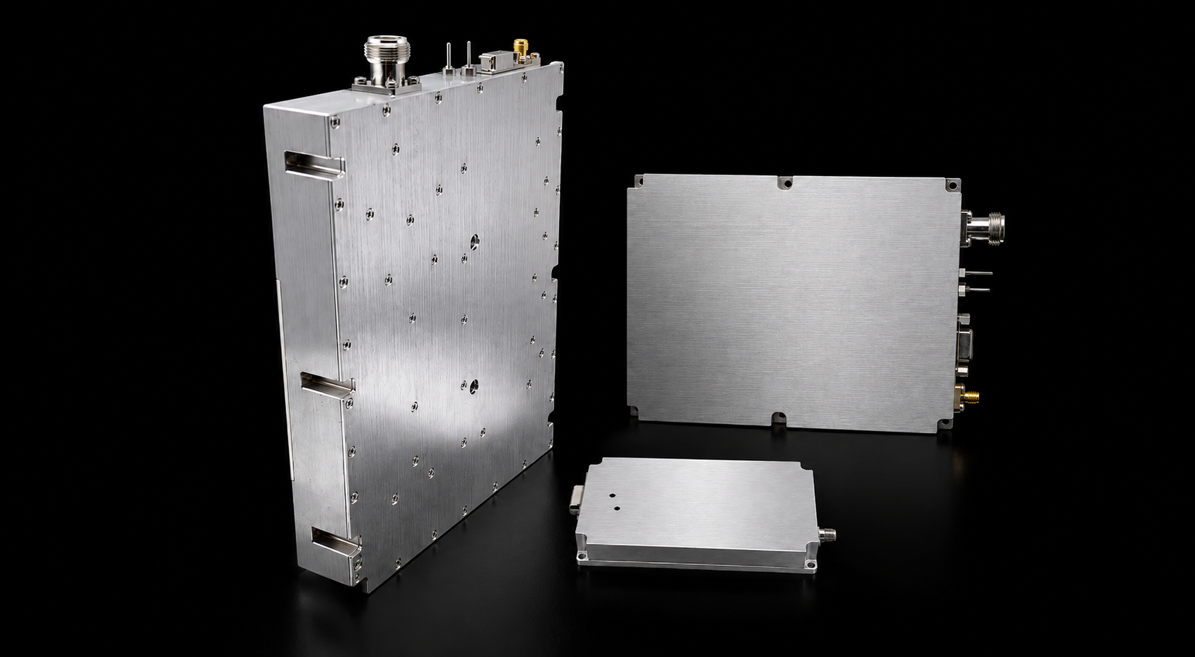
When reviewing RF Power Amplifier modules for C-UAS integration, buyers should ask how the GaN device is selected, mounted, cooled, screened, protected, and tested. The real question is not only whether the module uses GaN. The better question is whether that GaN device can stay stable under the load, heat, mismatch, and time that the field will create.
1. What Makes GaN Device Quality More Than a Label?
GaN Device Quality is more than a label because RF Power Amplifier reliability depends on the device’s hot-state behavior, not only its technology type. “GaN” tells you the transistor family; it does not prove the die, package, screening, or full-load behavior are suitable for long-term C-UAS operation.
Here’s the engineering point: two RF modules can both use GaN while showing different output drift, thermal rise, recovery behavior, and batch consistency. The difference often appears after the device is pushed beyond a short, clean bench condition.

What Should Buyers Avoid Assuming?
Buyers should avoid treating GaN as a shortcut for reliability. The device must still be judged by measurable behavior under stress.
Avoid relying only on:
- peak output power;
- GaN branding alone;
- one room-temperature test point;
- short pulsed output;
- center-frequency data;
- one sample module;
- price without screening evidence.
Key Takeaway: GaN Device Quality matters because the word “GaN” does not prove long-term full-load stability unless device behavior is verified under real stress.
| Buyer Assumption | Device-Level Reality | Better Review Point |
|---|---|---|
| GaN means reliable | Quality still varies | Screening and traceability |
| Peak power is enough | Hot-state drift may appear | CW stability curve |
| One sample proves design | Batches may differ | Batch comparison data |
| Protection solves risk | Device tolerance matters | GaN and protection fit |
A GaN-based amplifier should be approved by evidence, not by the technology label alone.
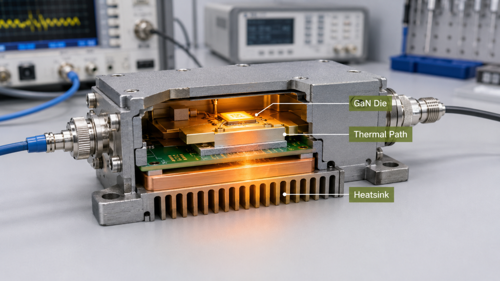
2. How to Judge GaN Device Quality by Thermal Data
GaN Device Quality affects full-load output because junction temperature controls drift, efficiency, gain stability, and degradation risk inside the RF transistor. If the GaN die runs too hot, the module may still function, but output stability and long-term margin can weaken.
The practical risk is clear: case temperature is not the same as junction temperature. A module housing may look acceptable while the GaN die is already operating close to a stressful hot-state condition.
What Thermal Data Matters at Device Level?
This section is not about general cabinet cooling. It is about the heat path from the GaN die into the package and module structure.
Ask for evidence around:
- junction temperature estimate or thermal model;
- package thermal resistance;
- die attach quality;
- hot-state output power;
- power drift after warm-up;
- thermal cycling behavior;
- device aging under long load.
Effective RF amplifier thermal management still matters, but GaN device thermal resistance decides how much stress reaches the core device before heat leaves the module.
Key Takeaway: Junction-level thermal behavior is a core GaN quality indicator because long-term full-load output depends on what happens inside the device, not only on the external heatsink.
| Thermal Item | Why It Matters | Weak Sign |
|---|---|---|
| Junction temperature | Sets device stress level | Output drift after warm-up |
| Package thermal resistance | Controls heat transfer | Local hotspot risk |
| Die attach | Affects heat spreading | Early thermal instability |
| Hot-state output | Shows real stability | Cold data looks better |
The strongest thermal review starts at the GaN die, then moves outward to PCB, housing, heatsink, and cabinet.
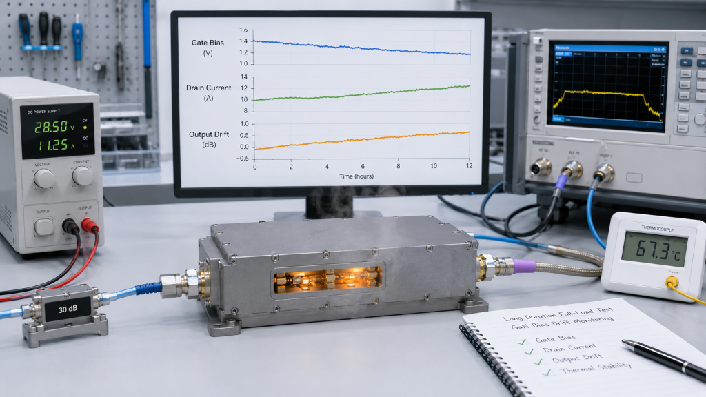
3. What Bias Drift Reveals About GaN Device Quality
GaN Device Quality can be judged through bias stability because RF Power Amplifier output depends on how the device behaves as temperature, drain current, gate bias, and operating time change. Bias drift can turn a stable cold module into a drifting hot module.
Here’s the useful distinction: this article is not only asking whether the amplifier reaches a wattage number. It asks whether the GaN device keeps its electrical operating point controlled after heat and time enter the system.
What Drift Signs Should Engineers Watch?
Device-level drift can appear gradually, especially during CW or high-duty operation. It may not create an immediate fault, but it can reduce repeatability and production confidence.
Watch for:
- Idq movement after warm-up;
- Vth drift over temperature;
- output power falling after heat soak;
- gain movement during long load;
- current change at the same RF output;
- different drift behavior between batches;
- slow recovery after cooling.
Key Takeaway: Bias drift reveals whether a GaN device remains electrically stable under full-load temperature and time, not only under cold-start testing.
| Drift Indicator | What It Suggests | What to Request |
|---|---|---|
| Idq movement | Bias instability | Hot-state current data |
| Vth shift | Device behavior change | Temperature comparison |
| Power drift | Output not settled | Power-versus-time curve |
| Batch drift spread | Inconsistent devices | Batch screening record |
A reliable GaN amplifier should hold a stable operating point after the device is hot, not only during startup.
4. How to Compare GaN Device Quality Across Batches
GaN Device Quality affects module reliability through batch consistency because the same RF Power Amplifier design must behave predictably across multiple production runs. One strong sample does not guarantee that later units will show the same thermal response, gain, drift, or mismatch tolerance.
This is where procurement should be careful. In multi-module C-UAS systems, batch variation can create unequal channel output, different warm-up behavior, different alarm timing, and more difficult troubleshooting.

What Batch Evidence Should Be Requested?
Batch consistency should be supported by repeatable test records, not verbal assurance. The goal is to know whether production modules behave close enough for system integration.
Ask for:
- swept-frequency output spread;
- gain spread across units;
- hot-state power comparison;
- current draw comparison;
- protection trigger behavior;
- burn-in pass criteria;
- serial-number test records.
General RF Power Amplifier reliability includes system-level stability, but this section focuses on how GaN device variation becomes production reliability risk.
Key Takeaway: GaN batch consistency helps ensure that one approved design remains stable across later deliveries, not only in the first sample.
| Batch Item | System Impact | Review Method |
|---|---|---|
| Output spread | Uneven RF channels | Unit-to-unit test data |
| Thermal spread | Different hot behavior | Hot-state comparison |
| Alarm timing | Inconsistent protection | Trigger behavior records |
| Current spread | Power budget variation | Full-load current data |
For batch procurement, repeatability is often as important as peak performance.
5. What Protection Behavior Says About GaN Device Quality
GaN Device Quality shapes protection behavior because RF Power Amplifier protection logic reacts to stress that the device must first survive or tolerate. VSWR, reflected power, temperature, voltage events, and current density all interact with the GaN transistor before the system reports a clean alarm.
Here’s the key difference from a protection-logic article: protection logic describes what the module does during a fault. GaN quality helps decide how much stress the device can tolerate before, during, and after that fault.
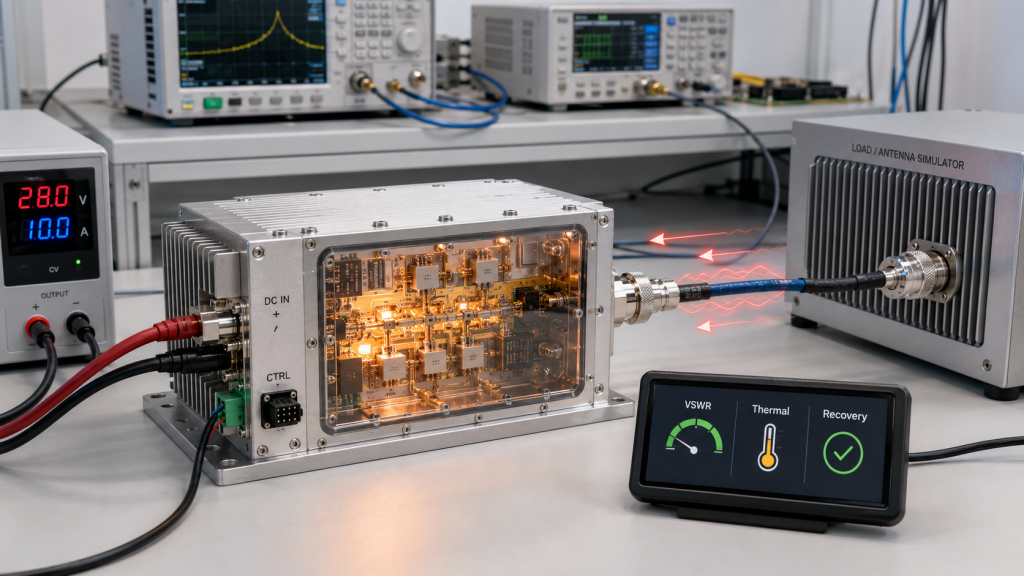
What Must Be Matched With GaN Tolerance?
Protection settings should be aligned with the real device margin. A weak device may require conservative thresholds, while a stronger and well-cooled device may operate more predictably under mild mismatch.
Review the coordination between:
- reflected-power tolerance;
- VSWR trigger threshold;
- thermal headroom;
- drain current stress;
- voltage event handling;
- recovery after mismatch;
- alarm visibility to the controller.
The way RF Power Amplifier protection logic responds to VSWR, temperature, voltage, and recovery conditions should be reviewed together with GaN device tolerance.
Key Takeaway: Protection is strongest when GaN tolerance, trigger thresholds, recovery behavior, and controller visibility are designed as one system.
| Stress Condition | GaN Quality Role | Protection Role |
|---|---|---|
| High VSWR | Tolerates reflected stress | Reduces or shuts output |
| Heat rise | Maintains stable operation | Prevents unsafe temperature |
| Voltage event | Handles electrical stress | Reports abnormal input |
| Fault recovery | Returns without drift | Restarts predictably |
Protection logic cannot turn weak GaN quality into strong field reliability; it must work with real device margin.
6. Why Do Real Loads Expose Weak GaN Faster?
GaN Device Quality becomes more visible under real loads because RF Power Amplifier field operation combines heat, duty cycle, antenna mismatch, supply variation, and frequency-dependent stress. These conditions are harder than a short 50-ohm dummy-load test.
Here’s the field reality: C-UAS cabinets, fixed-site RF platforms, and multi-channel systems rarely operate in ideal laboratory conditions. A GaN device that looks stable in a short test may show drift after hot operation, long feeder mismatch, or simultaneous channel loading.

What Field Conditions Stress GaN Devices?
Real installation adds stress from several directions at once. This is where device-level quality becomes system-level behavior.
Common stress factors include:
- True CW or high-duty operation;
- band-edge operation;
- imperfect antenna VSWR;
- outdoor cabinet heat;
- shared 28V rail loading;
- multi-module heat stacking;
- carrier switching;
- long feeder paths.
Existing duty-cycle guidance explains why operating time changes amplifier stress. For GaN review, the key point is that RF Power Amplifier duty cycle turns device quality into a continuous thermal and electrical requirement.
Key Takeaway: Real loads expose weak GaN faster because field stress combines thermal, electrical, RF load, and operating-time pressure.
| Field Factor | Device-Level Effect | Possible Symptom |
|---|---|---|
| High duty cycle | Heat accumulates | Output drift |
| Antenna mismatch | Reflected stress rises | Protection events |
| Band edge | Matching stress changes | Uneven output |
| Shared supply | Bias condition shifts | Power instability |
A GaN module should be validated against the load profile the field will create, not only the load the bench makes convenient.
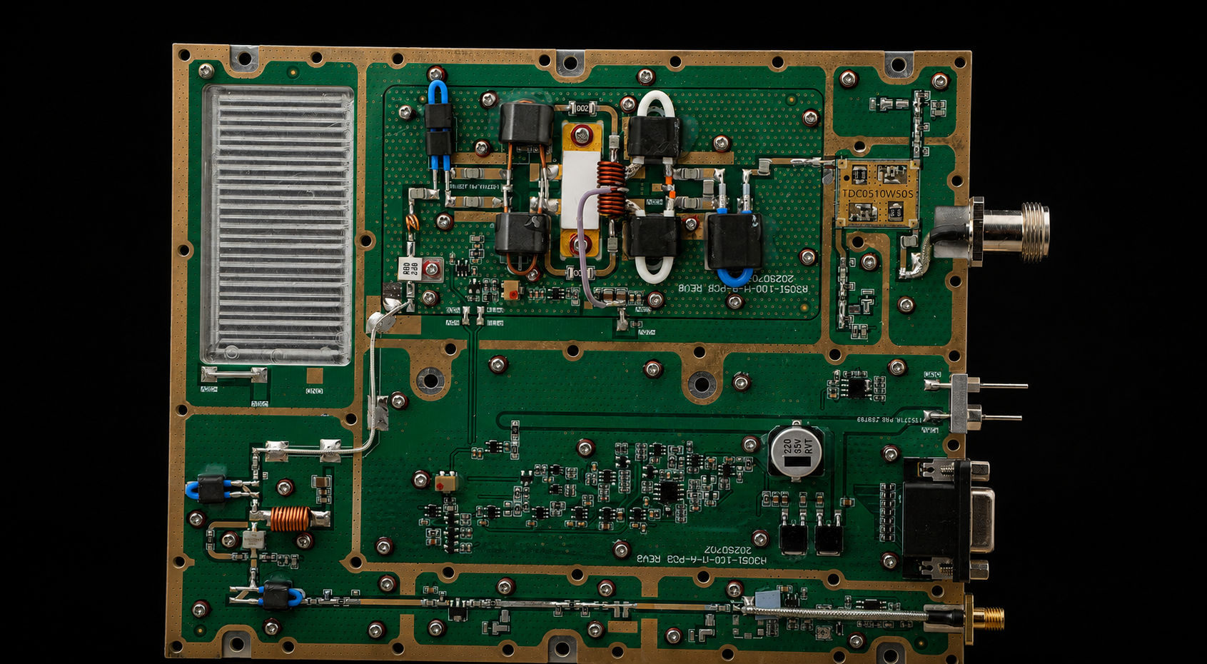
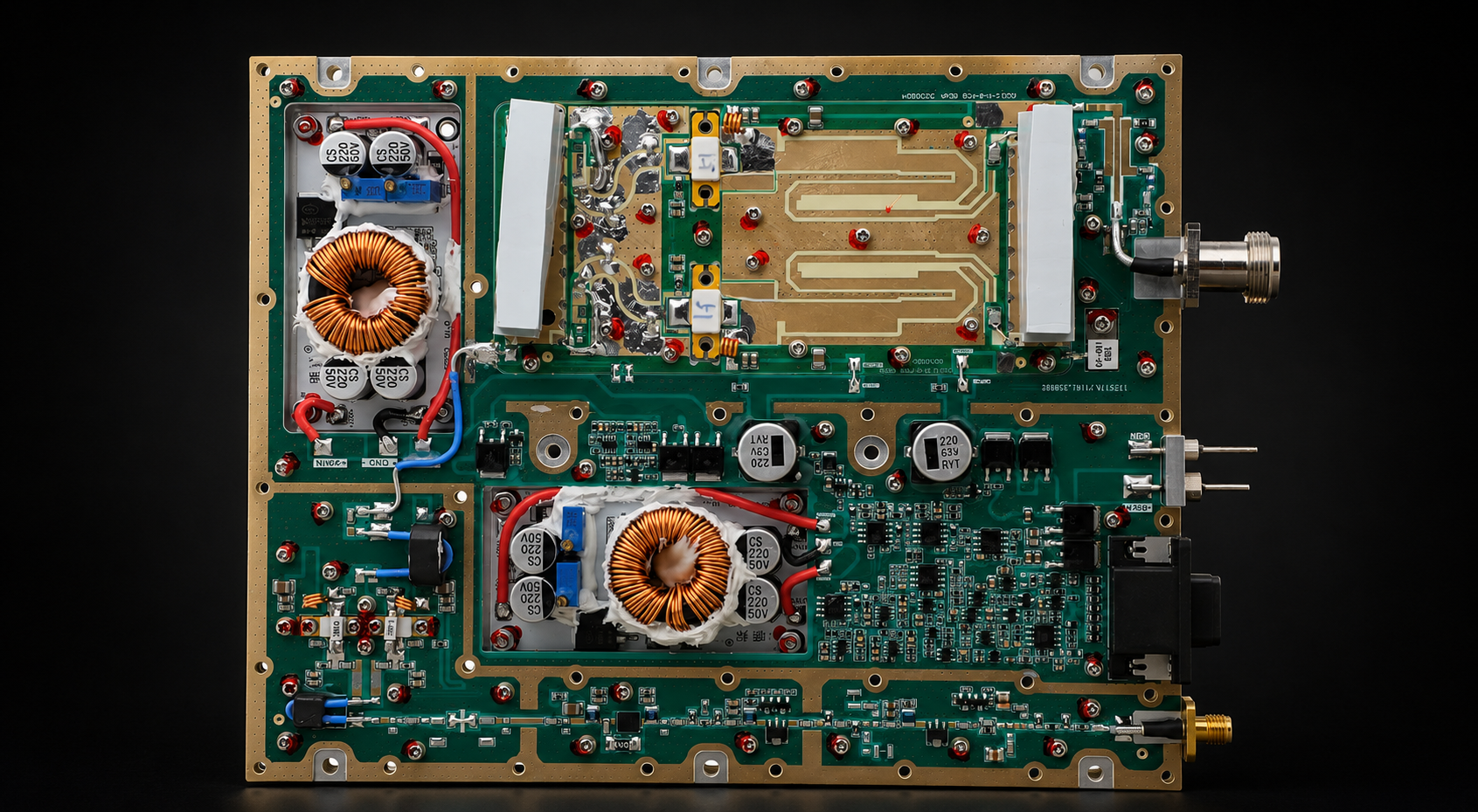
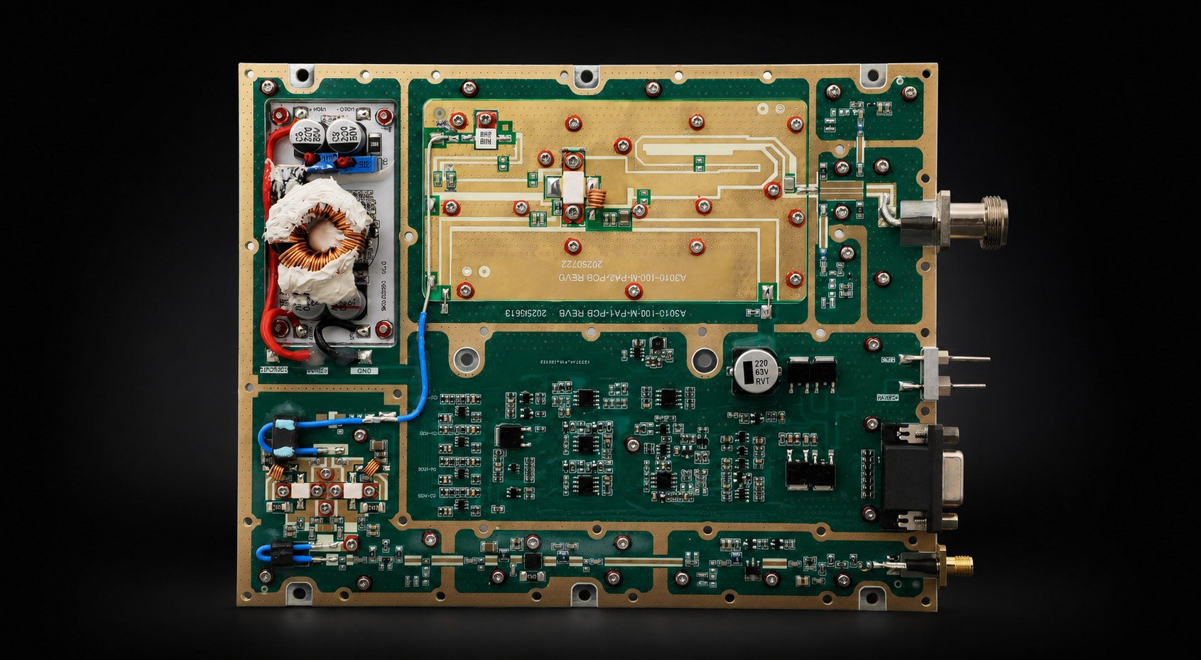
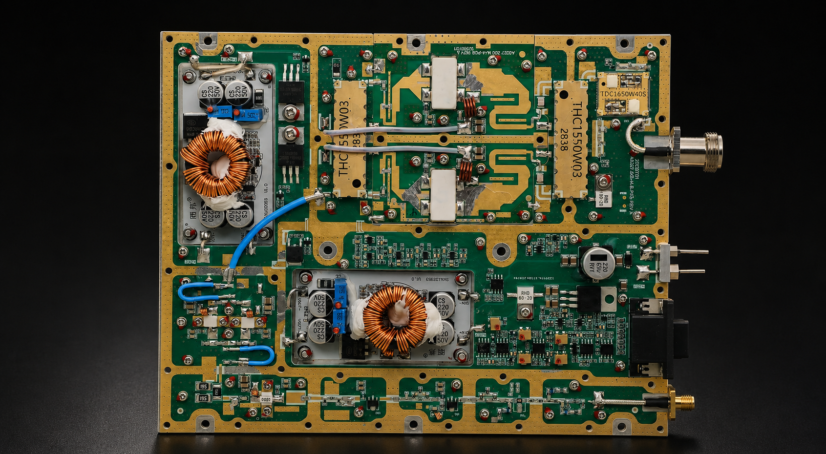
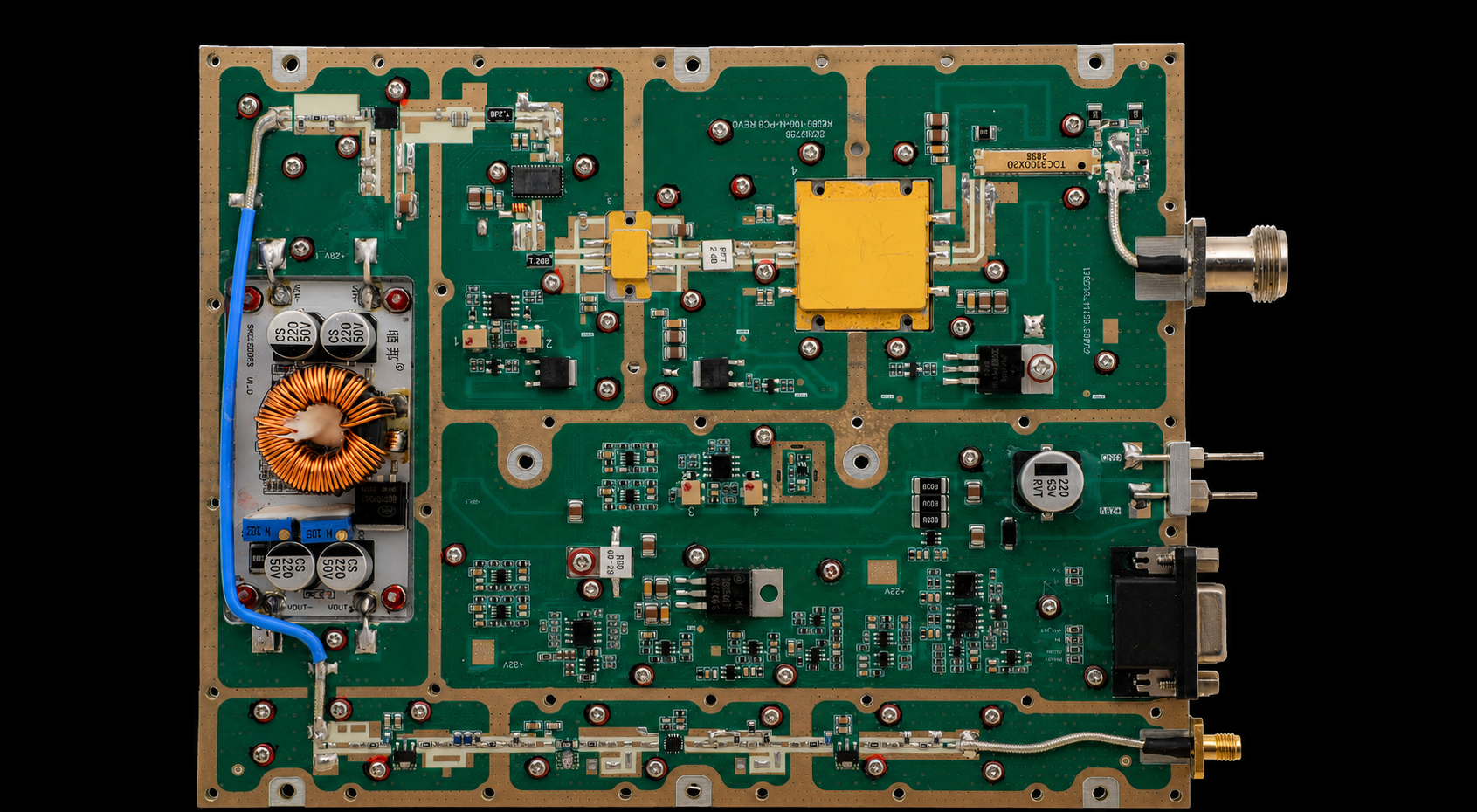
7. How Do PCB and Package Choices Support GaN Quality?
GaN Device Quality can only support RF Power Amplifier reliability when PCB layout and package integration control heat, current, grounding, parasitic inductance, and RF stability. A good GaN die can still perform poorly if the surrounding structure creates thermal or electrical stress.
This is where the article must stay device-focused. The topic is not general PCB design; it is how PCB and package choices allow the GaN device to maintain stable full-load behavior.
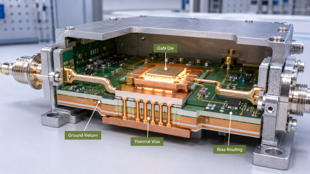
What Design Details Matter Around GaN?
The layout must help the device remove heat and maintain stable RF behavior. Weak local design can create drift, oscillation risk, uneven heating, and poor repeatability.
Check these details:
- die attach and package contact;
- low thermal resistance PCB structure;
- copper thickness and heat spreading;
- via placement near hot zones;
- low-inductance ground return;
- stable bias routing;
- RF output matching stability;
- housing contact flatness.
Key Takeaway: GaN quality is only useful when PCB, package, grounding, and thermal paths allow the device to operate within a stable electrical and thermal window.
| Design Area | Device Risk if Weak | Better Engineering Goal |
|---|---|---|
| Die attach | Hotspot or void risk | Consistent heat transfer |
| Ground return | RF instability | Low-inductance path |
| Bias routing | Drift or oscillation | Stable operating point |
| Housing contact | Poor conduction | Repeatable thermal contact |
The GaN device and its local environment should be judged together, not separately.
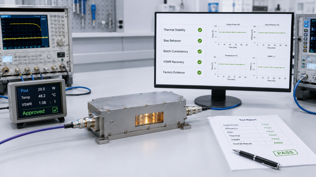
8. How Should Factory Verification Prove GaN Quality?
GaN Device Quality should be proven through factory verification that connects device screening, hot-state testing, mismatch behavior, full-band output, burn-in, and serial-number traceability. A single bench result cannot prove device-level reliability.
Here’s the practical risk: if factory testing only confirms a cold output number, it may miss thermal drift, batch spread, band-edge weakness, and protection recovery behavior. A stronger process makes GaN quality visible through repeatable evidence.

What Verification Should Be Included?
Factory verification should show how the module behaves when device stress is realistic. This is especially important for wideband and long-duty systems.
Useful checks include:
- incoming device screening;
- batch comparison;
- full-band swept output;
- CW or high-duty load testing;
- hot-state retesting;
- VSWR or reflected-power behavior;
- temperature and voltage protection response;
- serial-number-based reports.
Your site already discusses why full-band testing should measure output, gain trend, reflected behavior, efficiency, and temperature across low, middle, and high points. For GaN quality, that same testing should be read as device-stress evidence, not only module-level performance data.
Key Takeaway: Factory verification proves GaN quality when it shows repeatable hot-state, full-band, mismatch, and batch behavior.
| Verification Step | What It Reveals | Why It Matters |
|---|---|---|
| Device screening | Incoming variation | Reduces batch risk |
| Hot-state test | Thermal stability | Confirms real load behavior |
| VSWR test | Mismatch response | Supports field reliability |
| Serial report | Traceability | Helps batch review |
GaN quality becomes credible when the factory can show how it behaves under repeatable stress conditions.
9. How to Request GaN Device Quality Data Before RFQ
GaN Device Quality should be discussed before quotation because RF Power Amplifier reliability cannot be judged from frequency, wattage, and price alone. A supplier who cannot discuss device-level stability may not be ready for long-duty or mission-critical RF integration.
This is where the RFQ should become more specific. You do not need every semiconductor detail, but you should ask for the engineering evidence that affects full-load operation.

What Should the RFQ Ask For?
A GaN-focused RFQ helps separate short-output claims from long-term reliability evidence.
Request:
- GaN device screening approach;
- CW versus pulsed output behavior;
- hot-state output curve;
- batch consistency data;
- VSWR tolerance behavior;
- protection recovery behavior;
- burn-in or aging process;
- PCB and package thermal strategy;
- full-band test report;
- serial-number traceability.
Key Takeaway: A GaN-focused RFQ helps buyers compare device-level reliability instead of only comparing rated wattage.
| RFQ Question | Weak Reply | Stronger Reply |
|---|---|---|
| What GaN is used? | Brand only | Screening and process evidence |
| Can it run CW? | Simple yes | Hot-state CW data |
| Is it repeatable? | One sample result | Batch test spread |
| How is it protected? | Feature list | Trigger and recovery data |
The best RFQ asks how stable the GaN device remains, not only how much output the module can reach.
10. How Should GaN Device Quality Guide Final Selection?
GaN Device Quality should guide final RF Power Amplifier selection by connecting device thermal stability, bias behavior, batch consistency, mismatch tolerance, local PCB support, protection coordination, and factory verification. Rated power is only one part of the decision.
Here’s the decision logic: a good GaN amplifier is not defined by the word GaN. It is defined by whether the device and module design can stay stable under the target band, duty cycle, cabinet heat, antenna load, and procurement batch requirement.
What Decision Framework Should You Use?
A practical selection framework should move from device evidence to system risk. That keeps the review focused and avoids overvaluing one attractive data point.
Use this sequence:
- define frequency range and duty cycle;
- request hot-state output data;
- review junction and thermal path assumptions;
- compare CW and pulsed behavior;
- check batch consistency;
- review VSWR tolerance;
- review protection recovery;
- check PCB and package support;
- confirm burn-in and serial reports;
- discuss field stress with the factory.
As an RF Power Amplifier module and C-UAS core component source factory, RF SKYPOWER can help integrators review GaN device quality, thermal path, protection behavior, batch consistency, and long-term performance evidence before final module approval.
Key Takeaway: GaN Device Quality should be judged by stable full-load evidence, not by technology labels, short tests, or a single peak wattage value.
| Decision Area | What to Confirm | Why It Matters |
|---|---|---|
| Thermal stability | Hot-state behavior | Protects continuous output |
| Bias behavior | Drift under heat | Improves repeatability |
| Batch consistency | Unit-to-unit stability | Supports procurement |
| Factory evidence | Traceable testing | Reduces field risk |
The final selection should prove that the GaN device can survive the operating condition the system will actually create.
FAQ
Can I choose a GaN RF Power Amplifier by wattage alone?
No. Wattage only shows one output target. You should also review GaN thermal stability, bias drift, batch consistency, VSWR tolerance, PCB support, protection behavior, and test evidence.
What’s the best sign of good GaN Device Quality?
The best sign is stable hot-state performance under CW or high-duty operation. Batch consistency, mismatch behavior, and traceable test reports should support that result.
How do I know if GaN batch consistency is reliable?
You know by reviewing repeated unit data, not one sample result. Look for output spread, gain behavior, hot-state current, protection response, and serial-number reports across batches.
Can protection logic compensate for weak GaN quality?
No. Protection logic can reduce damage risk, but it cannot replace poor thermal stability, weak mismatch tolerance, or inconsistent device behavior.
What should I ask before approving a GaN module?
Ask for CW versus pulsed output, hot-state power curve, batch consistency, VSWR response, protection recovery, PCB thermal strategy, burn-in process, and serial-number test reports.
Conclusion
GaN Device Quality is a core factor in RF Power Amplifier reliability because full-load operation depends on what happens inside the device under heat, current, mismatch, frequency stress, and time. A module can reach rated output in a short test and still lack the device margin needed for stable CW operation, repeatable batch production, or real antenna-load stress.
For system integrators, RF engineers, and procurement reviewers, the practical lesson is clear: do not treat GaN as a label. Review junction-level thermal behavior, bias drift, batch consistency, mismatch tolerance, PCB and package support, protection coordination, and factory verification before approving a long-duty RF module.
RF SKYPOWER supports GaN-based RF Power Amplifier module selection by connecting device quality, thermal structure, protection logic, batch screening, and repeatable test evidence into one engineering review. If your project needs to compare GaN reliability before procurement, you can contact us today to discuss full-load RF module requirements with a source-factory engineering team.
Reliable C-UAS RF output is not built by choosing GaN as a label; it is built by proving that the GaN device can stay stable under the heat, mismatch, duty cycle, and time that the field will create.