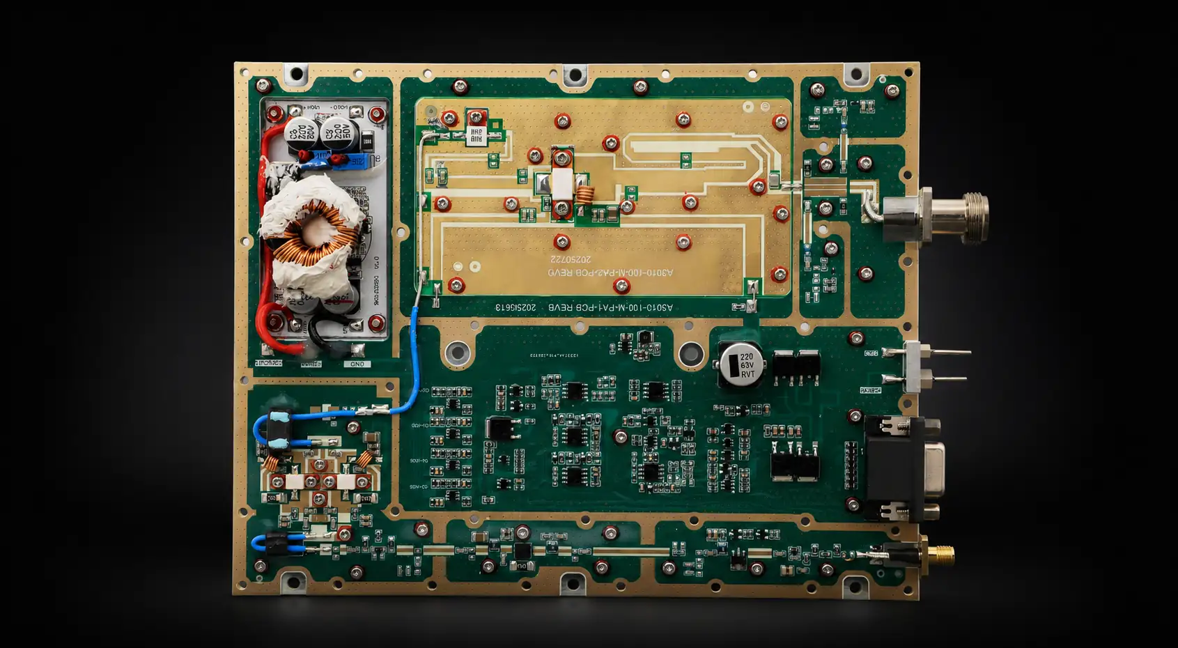
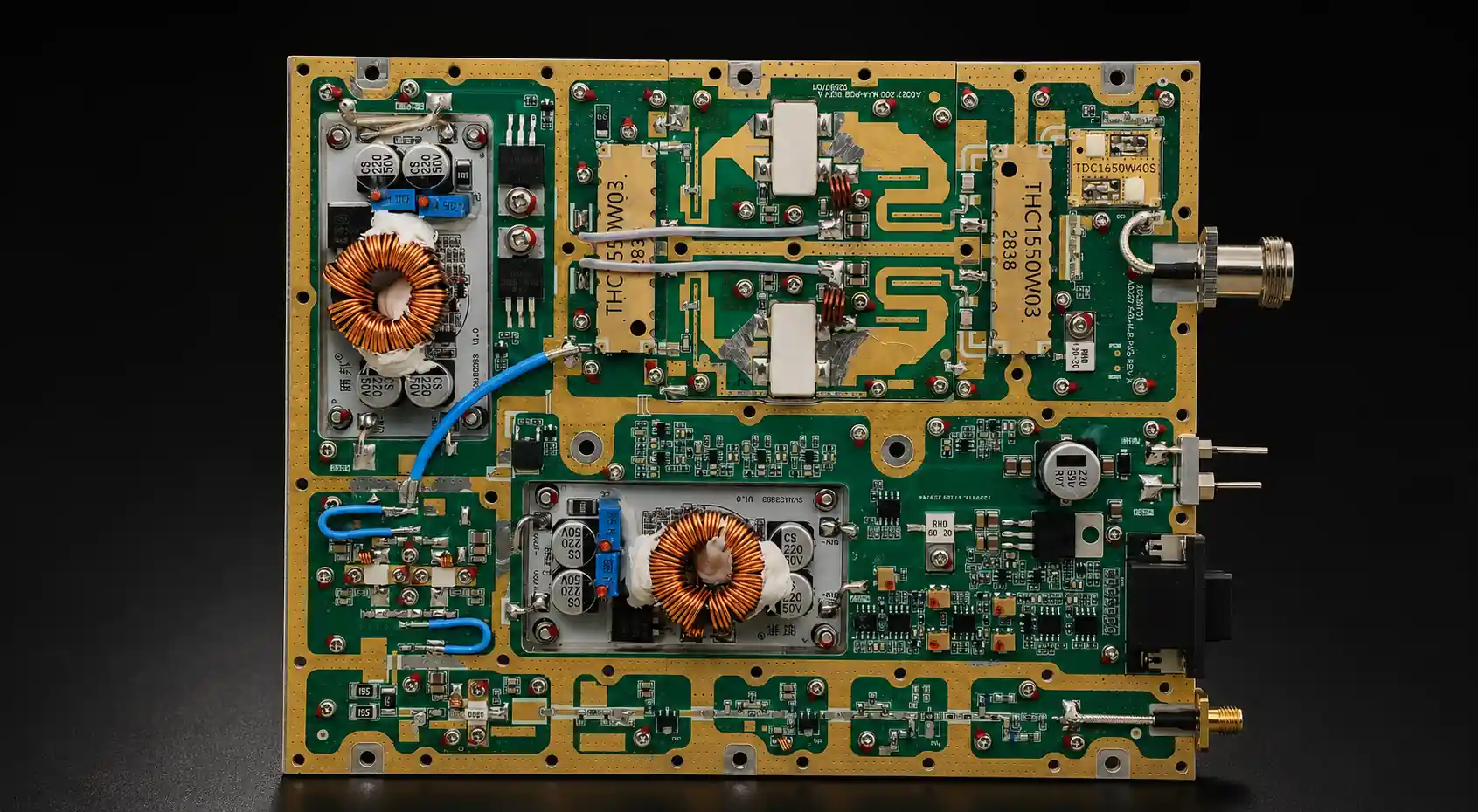
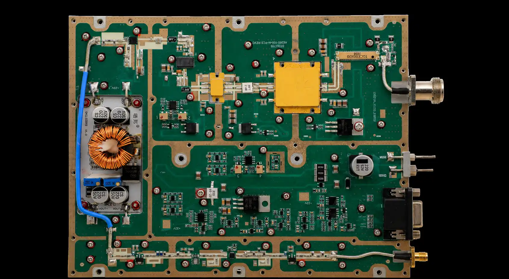


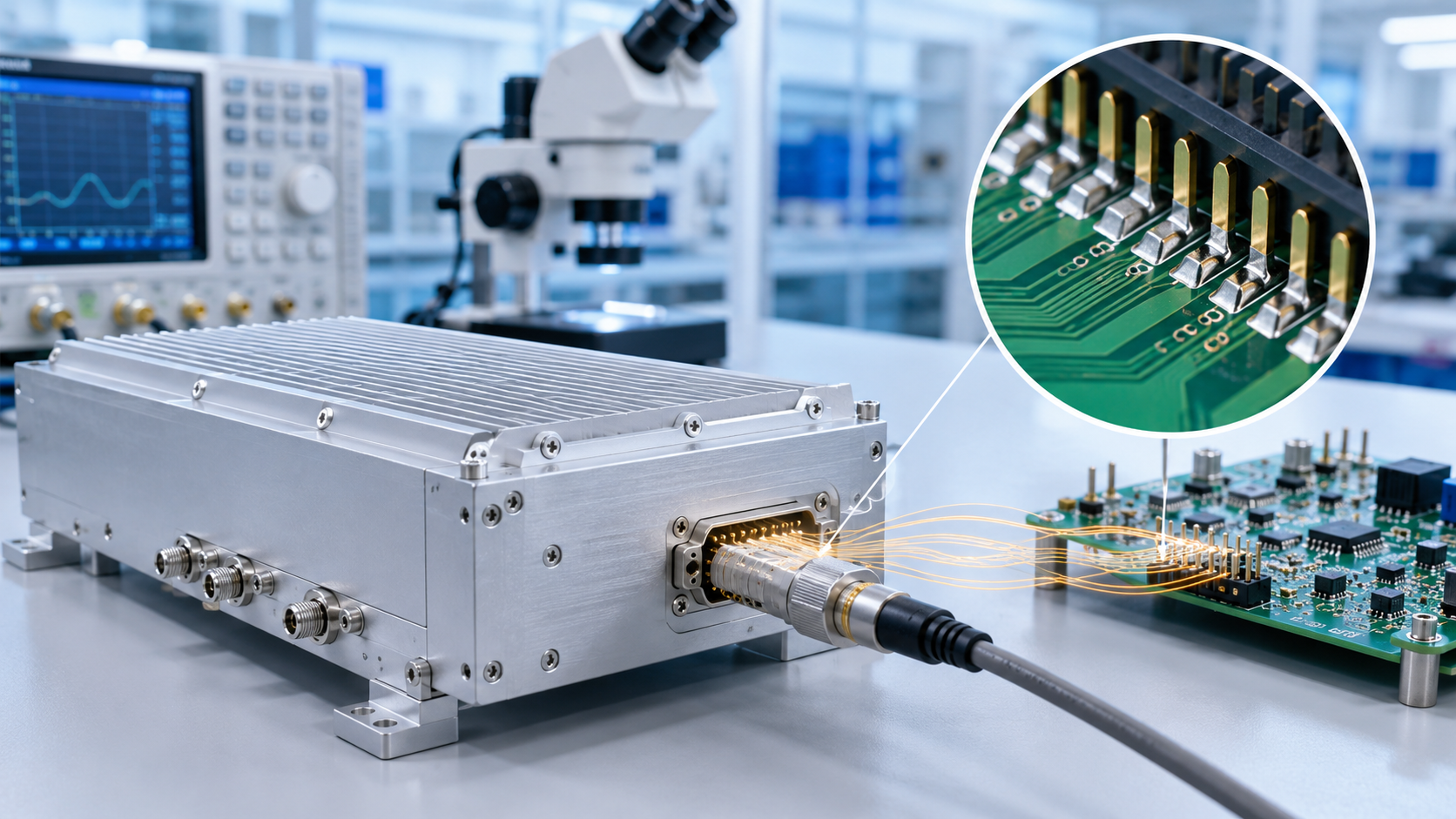
RF PA interface soldering may pass visual inspection and basic continuity while still causing intermittent Enable, Alarm, Status, or communication faults after connector loading, vibration, thermal change, or service handling.
Those symptoms do not prove that soldering is the root cause. External harness faults, poor connector mating, incorrect signal polarity, grounding differences, controller timing, PCB traces, and software states can produce similar behavior. Approval must therefore separate solder-joint evidence from the rest of the control path.
Before choosing custom RF Power Amplifier modules, define the critical interface pins, workmanship criteria, connector support, permitted rework, approved stress boundary, and functional signals that must remain stable before and after testing.
1. What Interface Soldering Can—and Cannot—Explain
A soldered interface provides the electrical connection between the PCB and a connector, pin, wire, or terminal. A weak joint may create:
- Intermittent command response
- Missing alarm or status feedback
- Communication dropouts
- Unstable sensing signals
- Stress-sensitive continuity
- Failure after handling
However, the same symptoms can originate elsewhere.
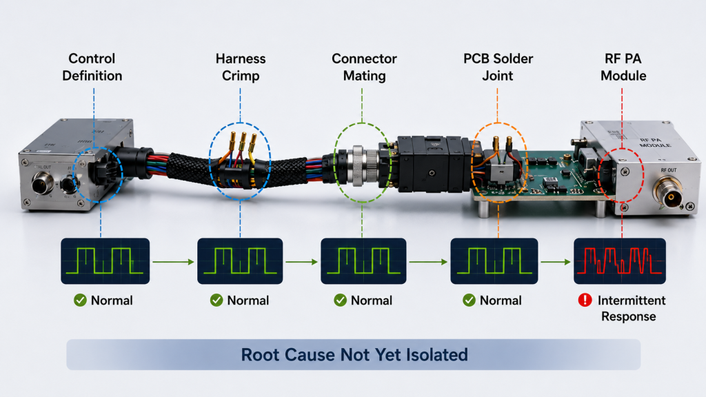
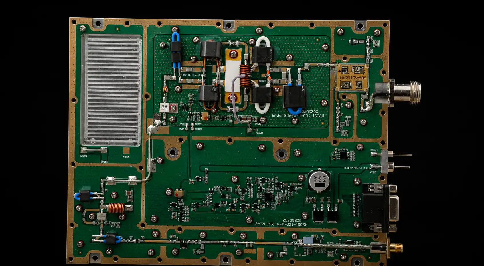
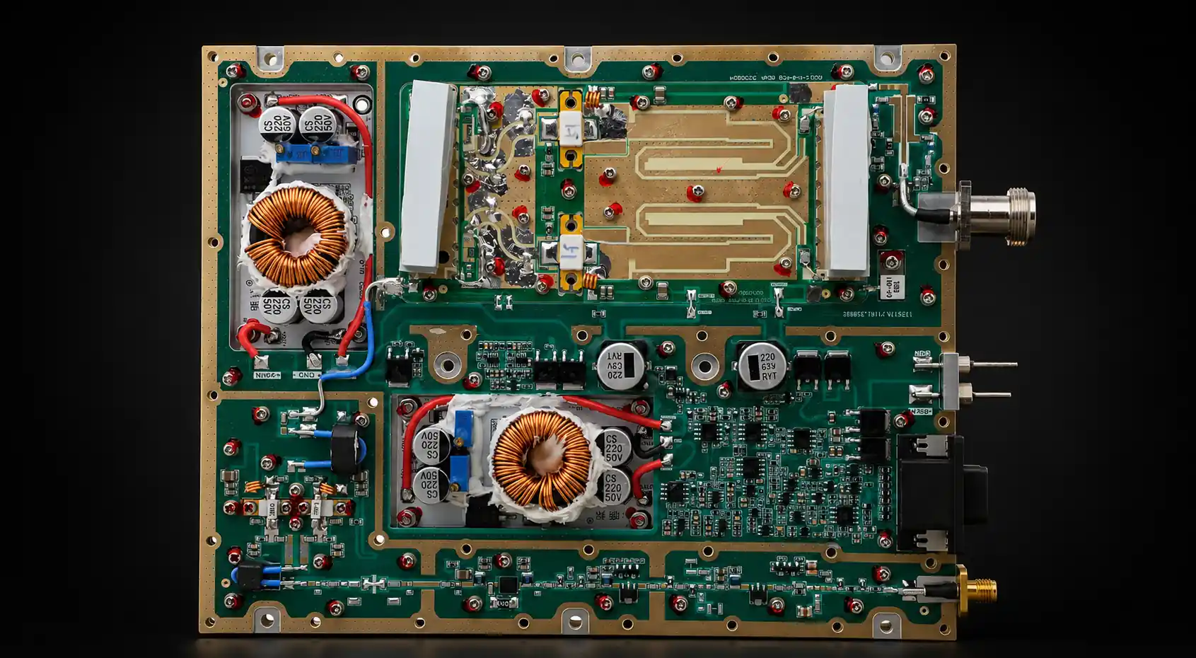
PCB solder-joint faults
Possible assembly faults include:
- Insufficient wetting
- Nonwetting or dewetting
- Solder bridges
- Cracked joints
- Lifted pads
- Pin misalignment
- Incomplete through-hole fill where applicable
- Rework damage
- Electrically significant contamination
Connector mating faults
The PCB joint may be acceptable while the mating interface is unstable because of:
- Bent contacts
- Incomplete insertion
- Loose locking hardware
- Housing misalignment
- Contact wear
- Poor terminal retention
Harness crimping faults
External harness problems can include:
- Weak conductor crimps
- High contact resistance
- Poor pull strength
- Insufficient strain relief
- Terminals not locked into the housing
Control-definition faults
The physical interface may also be blamed incorrectly when the actual issue is:
- Wrong active polarity
- Floating input
- Incorrect pull-up or pull-down
- Wrong voltage level
- Timing mismatch
- Wrong device address
- Software-state error
- Incorrect pin mapping
Evidence Boundary: Intermittent control behavior can justify a solder-joint inspection, but it does not prove soldering is the root cause until the harness, connector mating, ground reference, signal definition, controller behavior, and PCB interface have been separated.
A stress-sensitive dropout is a reason to inspect the soldered interface. It is not proof that the solder joint caused the fault.
2. Which Joints and Mechanical Loads Need Review
The inspection method should match the interface construction.
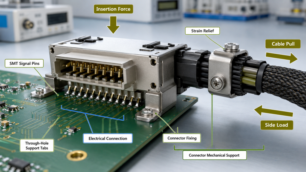
SMT connectors
Surface-mounted connectors should be reviewed for:
- Pad alignment
- Solder wetting
- Coplanarity
- Bridge risk
- Pad condition
- Mechanical fixing
A surface-mounted connector should not rely on solder alone to absorb repeated insertion or side loading when the design requires additional support.
Through-hole connectors
Through-hole interfaces may require checks for:
- Pin alignment
- Connector seating
- Hole and pad condition
- Required solder fill
- Wetting
- Cracks
- Bridges
The acceptance boundary should match the actual connector and process rather than using one generic rule for every joint.
Hand-soldered wires or terminals
Check:
- Conductor preparation
- Wetting
- Insulation clearance
- Exposed conductor length
- Heat damage
- Strain relief
- Rework history
The soldered connection should carry the electrical path, not the cable pull.
Workmanship and process condition
Useful evidence includes:
- Joint alignment
- Wetting condition
- Bridge or short risk
- Pad or PCB damage
- Connector seating
- Rework condition
- Approved cleaning or no-clean process
- Inspection record
Terms such as “cold solder joint” may be useful during troubleshooting, but formal approval should rely on observable conditions and defined criteria.
Visible flux residue does not automatically prove failure. The review should confirm whether the material, cleaning or no-clean process, inspection method, environmental boundary, and any later coating process remain controlled.
Likewise, a void or hidden feature should not automatically be rejected without considering the joint type, location, electrical role, mechanical load, and applicable acceptance criteria.
Mechanical support
Solder should provide the electrical connection. It should not become the primary structure carrying:
- Cable pull
- Connector insertion force
- Housing misalignment
- Repeated service load
- PCB bending
- Harness side load
Review connector fixing, housing alignment, strain relief, PCB support, harness routing, and service access. A visually acceptable joint may still fail when repeated mechanical load is transferred directly into the soldered pins.
3. How to Separate a Solder Fault from the Rest of the Control Path
Diagnosis should follow the signal path before solder rework begins.
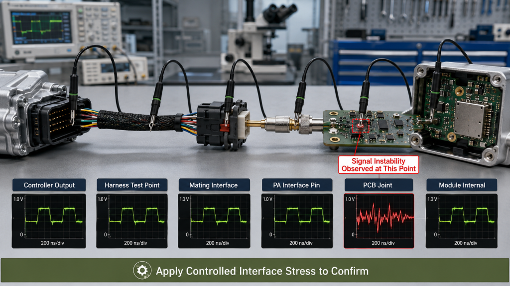
Use this sequence:
- Confirm the commanded operating state.
- Measure the controller output.
- Check the external cable and harness.
- Confirm connector mating and terminal retention.
- Measure the signal at the PA interface.
- Confirm the ground or reference condition.
- Compare expected and measured voltage levels.
- Repeat with another cable, controller, or module when appropriate.
- Apply only the approved connector, temperature, or vibration stress.
- Inspect the PCB joint when the fault follows the module-side interface.
General RF PA control-interface requirements should define voltage levels, active polarity, timing, addressing, alarm behavior, and communication conditions before soldering is blamed.
The external cable must also be isolated. Poor RF PA harness crimping can produce symptoms almost identical to a PCB-side solder fault.
RF PA Interface Fault Isolation Map
| Symptom | Check First | Soldering Evidence |
|---|---|---|
| Enable dropout | Polarity, logic level, cable | Fault follows repeatable module-side stress |
| Alarm jump | Alarm source, ground reference | One S/N changes under the same stress |
| Communication loss | Address, cable, protocol settings | Local interface changes with heat or insertion |
| Missing status | Pin map, source signal, connector | PCB-side signal becomes intermittent |
| Unstable feedback | Reference point, wiring, supply noise | Reading changes only at the module-side joint |
The result should identify where the signal becomes unstable. Otherwise, solder rework may appear to solve the problem temporarily while the real fault remains in the harness, connector, grounding, or control definition.
4. How to Test the Interface Before and After Stress
A useful acceptance test combines inspection, baseline function, defined stress, and repeatable retesting.
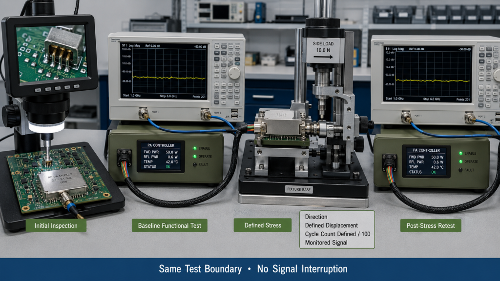
Step 1: Initial inspection
Check:
- Alignment
- Wetting and solder condition
- Bridge or short risk
- Cracks or lifted pads
- PCB damage
- Connector support
- Strain relief
- Rework condition
- Approved process state
Hidden or high-risk joints may require additional inspection when the interface construction, failure consequence, or project requirement justifies it.
Step 2: Baseline functional test
Test the supported command, alarm, status, and communication signals under a defined electrical boundary.
Record:
- Pin function
- Expected state
- Measured voltage or logic level
- Controller command
- Module operating state
- Cable and connector condition
- Result by S/N
Step 3: Defined stress
Project-approved stress may include:
- Connector insertion and removal
- Controlled side load
- Cable service handling
- Vibration
- Thermal exposure
- Cabinet installation load
- Repeated command cycling
An uncontrolled hand wiggle is a troubleshooting aid, not formal acceptance evidence.
A movement test should define:
- Direction
- Force or displacement
- Cycle count
- Powered or unpowered state
- Monitored signals
- Allowed interruption
- Pass/Fail condition
Vibration or thermal testing should identify the test profile, module state, installed harness, connector condition, monitored signals, and pre-stress baseline.
There is no single universal stress level for every RF PA interface. The profile must match the project and installation boundary.
Step 4: Post-stress retest
Repeat the same functional test and confirm:
- Same logic state
- Same voltage level
- Same communication response
- No intermittent dropout
- No new alarm
- No connector movement
- No visible damage
Where protection status is carried through the interface, check the physical signal path separately from the complete RF PA protection logic. A stable Alarm pin does not prove the entire protection sequence is correct, and a real protection event does not automatically prove the interface is faulty.
A joint is not approved only because it looks acceptable. Approval requires acceptable workmanship, adequate mechanical support, and stable signal behavior under the defined test boundary.
5. What Process, Rework, and S/N Records Must Remain Traceable
Interface reliability depends on repeatable manufacturing and controlled changes.
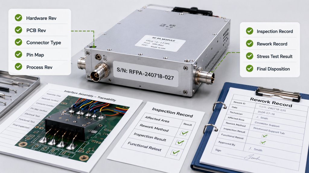
The record should connect:
- Module S/N
- Hardware and PCB revision
- Connector type
- Interface pin map
- Soldering process type
- Process revision
- Inspection date and station
- Rework history
- Cleaning or no-clean process state
- Mechanical support configuration
- Stress-test condition
- Pre-stress and post-stress results
- Final disposition
Process-change control
Changes that may affect interface behavior include:
- Connector supplier or finish
- PCB revision
- Soldering method
- Reflow or hand-soldering instruction
- Cleaning process
- Mechanical support
- Harness routing
- Housing tolerance
A change does not automatically indicate failure. It should trigger the review required by the project’s RF PA process-change control.
The supplier does not need to disclose every confidential manufacturing setting. The buyer needs evidence showing:
- Which process was approved
- Which revision was used
- Whether production matches that revision
- Whether a change occurred
- Whether the change was reviewed and retested
Rework control
A repaired interface is not automatically unacceptable.
It becomes a risk when:
- The method is undefined
- Pad damage is not assessed
- Cleaning is uncontrolled
- Mechanical support is not restored
- Functional testing is not repeated
- The rework is not linked to S/N
A controlled rework record should identify the reason, affected pin or connector, approved method, inspection result, functional retest, stress retest when required, and final disposition.
“Reworked and passed” is weaker than evidence showing what changed and how the interface was requalified.
6. What Should Approve, Review, or Hold the Interface?
The decision should combine workmanship, mechanical support, functional stability, process control, and traceability.
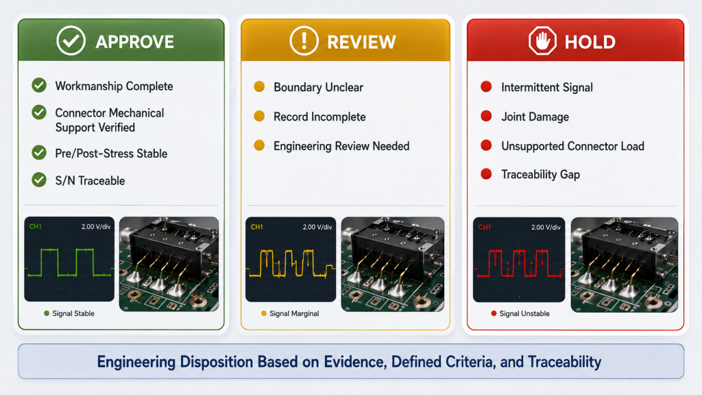
Approve
Approval is reasonable when:
- Workmanship criteria are satisfied.
- The connector is properly supported.
- No unapproved rework exists.
- Critical signals pass baseline and post-stress tests.
- Hardware and process revisions are traceable.
- The report matches the delivered S/N.
Review
Keep the interface in Review when:
- A cosmetic concern has no confirmed functional effect.
- Rework exists but one record is incomplete.
- The stress boundary is unclear.
- One signal is close to the accepted limit.
- Mechanical support needs engineering confirmation.
- A process change occurred but evidence is incomplete.
Review means engineering confirmation is required before release.
Hold
Keep the interface on Hold when:
- An intermittent signal is reproduced.
- A bridge, crack, lifted pad, or damaged joint is found.
- Unapproved rework is present.
- Connector load is carried mainly by soldered pins.
- Critical feedback cannot be verified.
- Hardware or process revision is untraceable.
- Pre-stress and post-stress results cannot be compared.
- The report is not linked to the delivered S/N.
Interface Soldering Approval Matrix
| Decision | Typical Condition | Action |
|---|---|---|
| Approve | Workmanship, support, tests, and traceability are complete | Release |
| Review | One boundary, change, or record needs confirmation | Engineering review |
| Hold | Intermittency, damage, unsupported loading, or traceability gap remains | Correct and retest |
The result should become part of the project’s C-UAS RF PA acceptance checklist. A control connector should not be accepted only because the module powers on. The record should prove that critical interface signals remain stable under the approved electrical and mechanical boundary.
Conclusion
The same interface symptom can come from soldering, connector mating, harness crimping, grounding, or control-definition faults. Root cause must be isolated before rework begins.
Approval requires:
- Acceptable workmanship
- Adequate mechanical support
- Stable pre-stress and post-stress behavior
- S/N-linked process and test evidence
RF SKYPOWER can support early engineering review for RF PA control-interface acceptance. Send the connector and pinout, signal definitions, PCB and hardware revision, expected mechanical and thermal stress, workmanship criteria, rework rules, functional test boundary, and required S/N-linked report format.
Contact RF SKYPOWER before one marginal solder joint, unsupported connector, or untraceable rework turns a stable factory test into an intermittent field-control fault.