
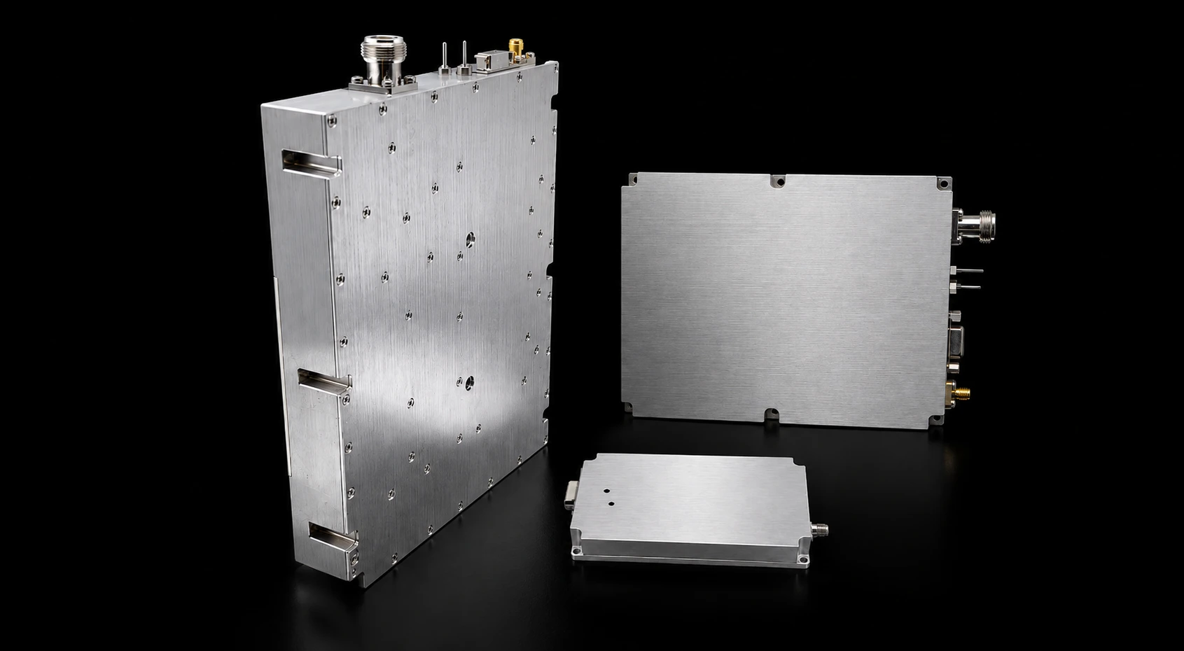
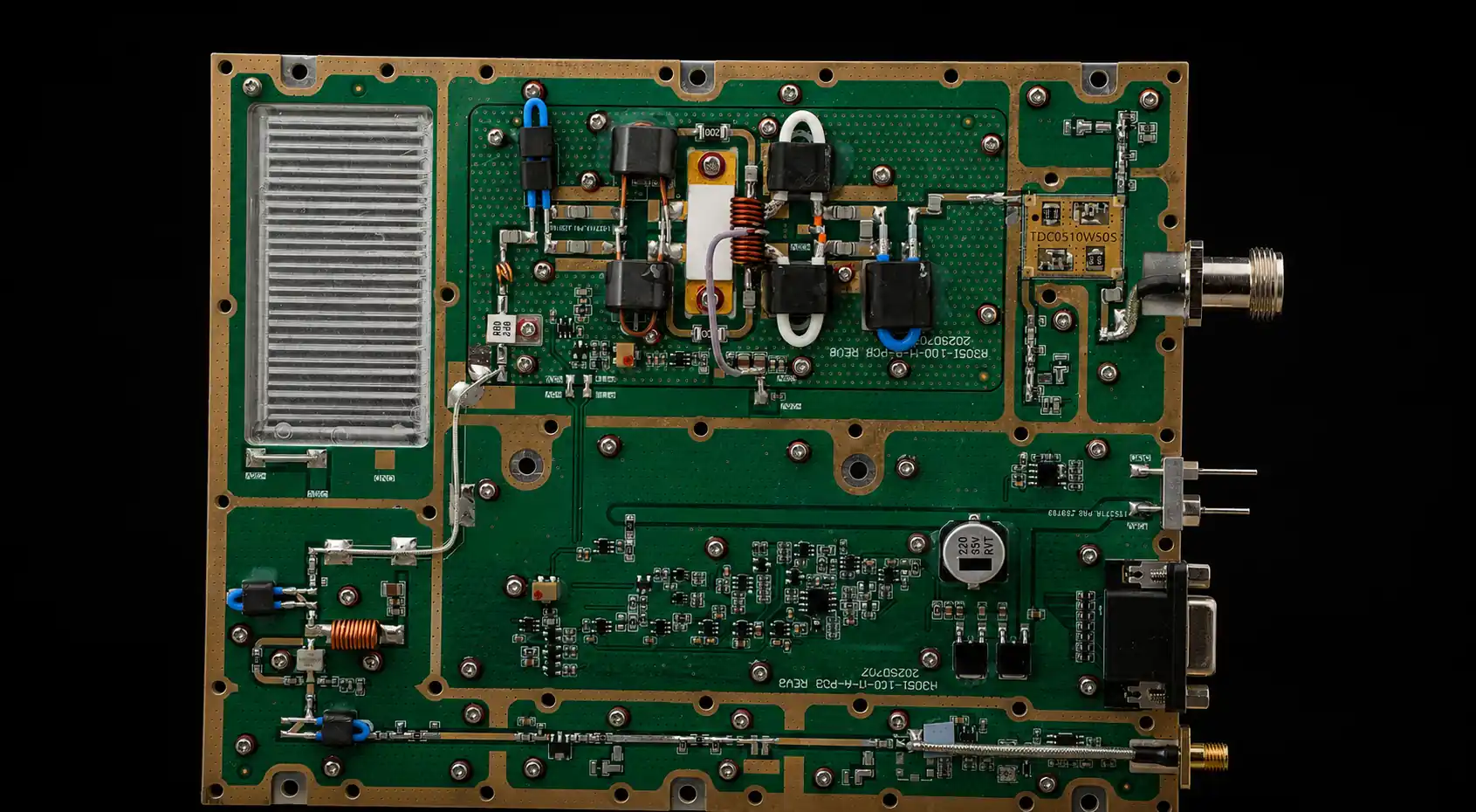
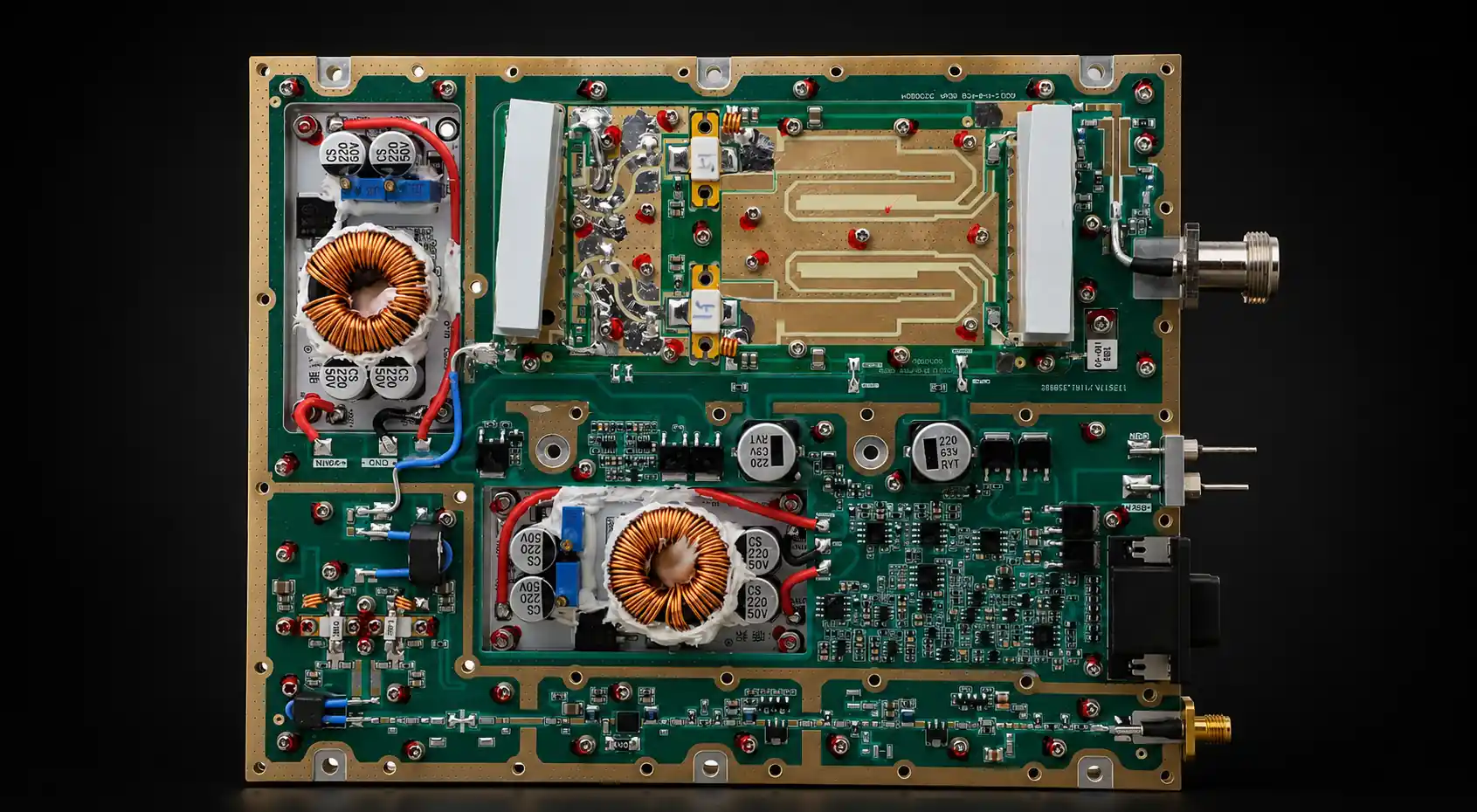
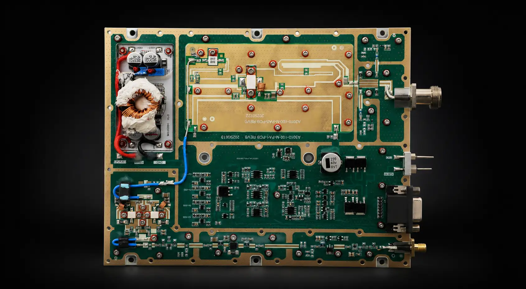
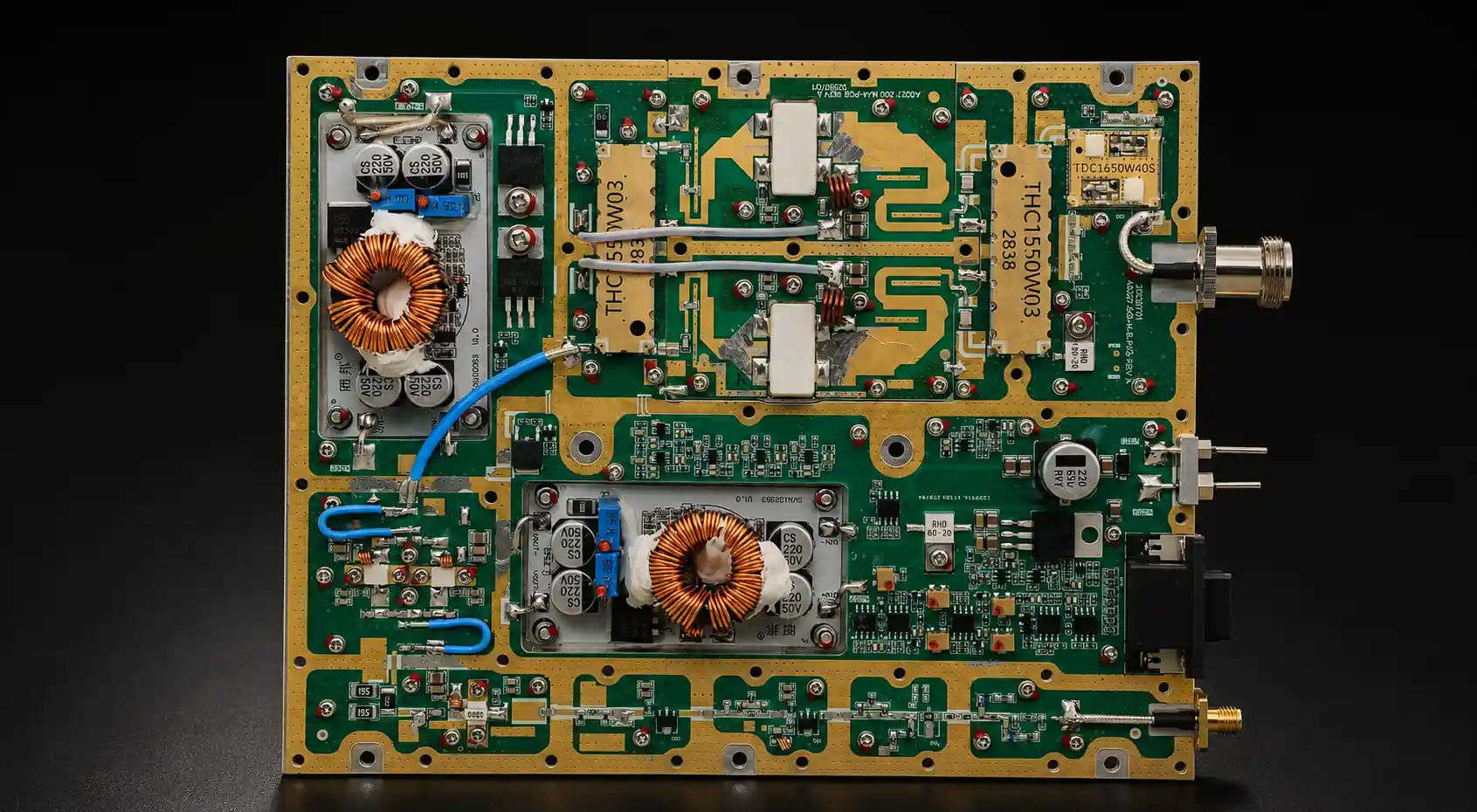
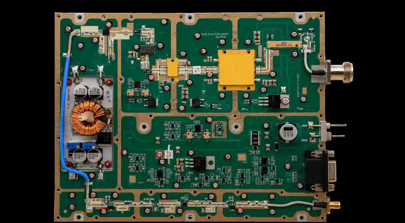
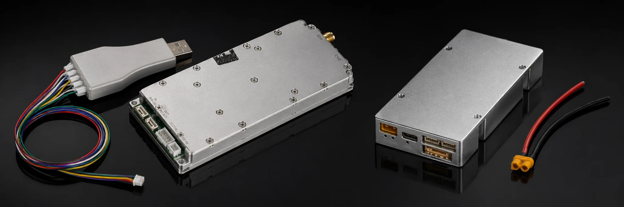


An RF amplifier DC input connector should be approved as a complete mated interface, with current capacity, contact loss, pin allocation, and mechanical retention supported under the intended operating conditions. A catalog ampere value or a connector that physically mates does not establish suitability; the evidence must match the module’s actual current, local temperature, loaded contacts, and positive-and-return path.
The key evidence gap is whether the rating and test conditions apply to the exact housing, contacts, terminals, wiring, and installation being considered. For C-UAS integration, an undefined interface can leave contact heating or module-terminal voltage loss undiscovered until the system is loaded. Start by fixing the mated configuration and pinout.
1. Lock the Complete DC Connector and Pinout
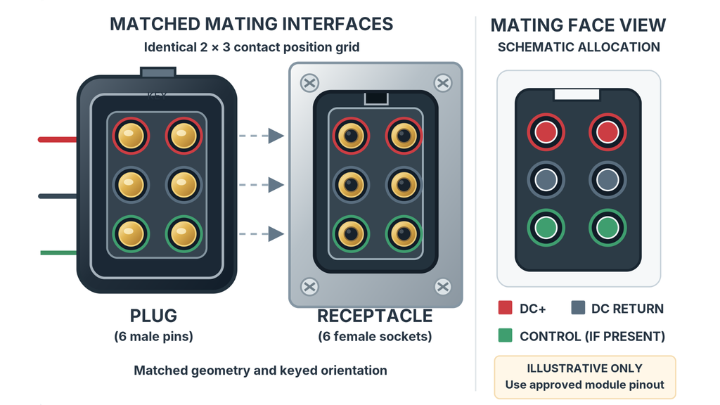
Qualification applies to the complete mated assembly. Record the manufacturer and part number for both mating halves, the contact or terminal part numbers and plating, the module interface revision, and the approved mating combination; family names or visual fit alone cannot establish compatibility.
The interface drawing should identify the view direction, keying and mating orientation, and each assigned cavity. Mark positive DC, the power return, and any control contacts separately. Do not assume that chassis, signal ground, and the DC return are interchangeable; use the approved module pinout for the power loop.
The buyer’s output from this step is a configuration record that another engineer can reproduce: exact parts and revisions, a pinout view, and the complete positive-and-return allocation. If any mating part, polarity, or view orientation is unresolved, hold approval and do not energize the connection. This interface decision sits within C-UAS module selection, but the broader module family does not establish the qualification of a particular connector combination.
2. Read Current Ratings at the Installed Thermal Condition
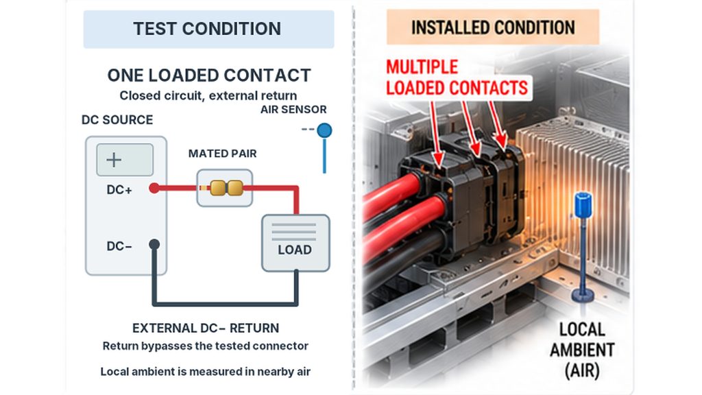
A connector current rating applies only with its stated test conditions. Check whether the rating describes one contact, a specified group of contacts, or the complete connector assembly, and whether the listed wire size, number and position of simultaneously loaded contacts, ambient temperature, and mounting or heat-transfer path match the proposed installation.
Use the module’s actual DC input current for the required operating state. RF output power divided by nominal DC voltage is not a substitute for the module input-current requirement. Define the maximum sustained input current over the project-approved module-terminal voltage and RF operating-state range. Identify the lowest qualified module-terminal voltage separately, and tie each value to its applicable duty cycle and test condition. Treat startup or other transient current separately, including its magnitude and duration.
The thermal evidence should apply to the installed arrangement. Define the local ambient temperature around the connector and evaluate both temperature rise above that local ambient and the component’s absolute temperature against the applicable limit. Nearby heat sources, PCB conduction, cable heat flow, and the number and location of loaded contacts can change the result. A cold, single-contact rating cannot automatically be carried over to a warm, multi-contact installation.
Request the applicable rating or derating basis, or condition-matched measurements for the actual assembly. If the rating conditions do not cover the installed configuration, do not treat the fact that the module powers on as proof of continuous current capacity.
3. Separate Contact Resistance From the Total Voltage-Drop Budget
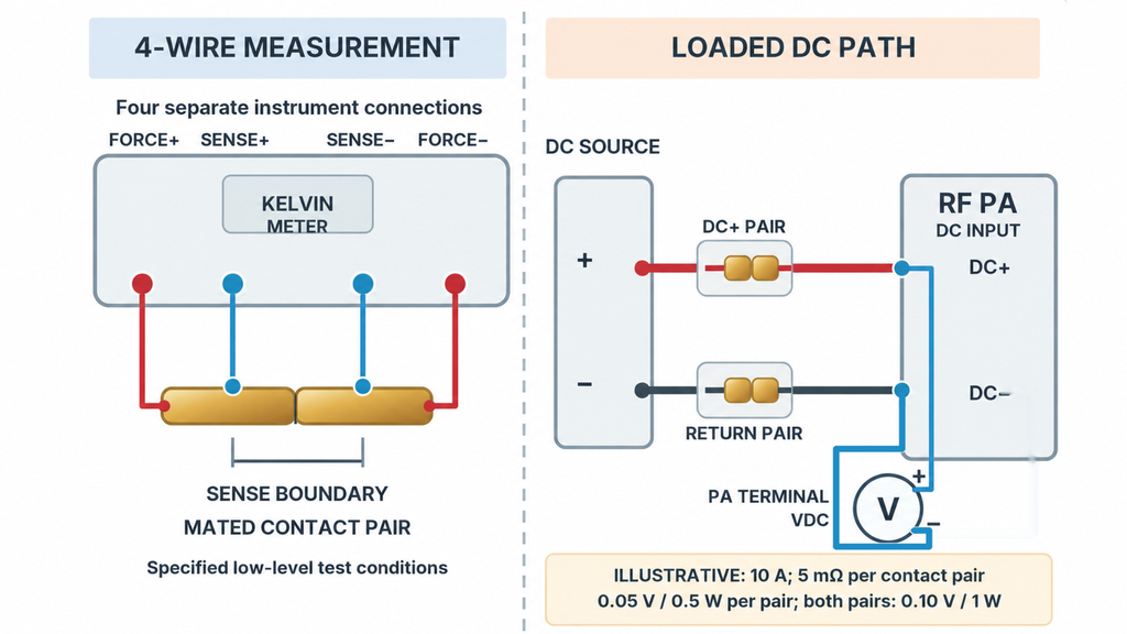
A low-level contact-resistance measurement, voltage drop under operating current, and temperature under load answer different questions. Before comparing results, define the measurement boundary: which mating contact pair is sensed, whether the measurement includes the crimp, wire, or PCB path, and where the voltage is measured relative to the module terminals.
For the low-level contact-resistance test, use the manufacturer’s specified test current and voltage with an appropriate four-wire measurement or other specified method to separate contact resistance from lead and fixture resistance. Then assess loaded voltage drop under the required current and temperature condition. Include both positive and return contacts in the complete path budget, while keeping the connector’s contribution separate from cable, crimp, and PCB losses. The allowable connector contribution must fit within the project-approved module-terminal voltage window; this article sets no universal resistance or voltage-drop limit.
For an illustrative resistive calculation only, 10 A through a defined mated contact pair with 5 mΩ resistance produces 0.05 V drop and 0.5 W dissipation at that pair. If the return contact pair has the same assumed resistance and carries the same 10 A loop current, both pairs together contribute 0.10 V and 1 W. These assumed values are not measurements, acceptance limits, or a temperature-rise prediction.
If the sense points, included resistance, or module voltage window is unknown, do not declare the contact acceptable or attribute the total loss to that contact alone. The complete conductor length and positive-and-return loop remain a separate DC cable voltage-drop budget; use that broader calculation when cable sizing or total path loss is the decision.
4. Qualify Parallel Power and Return Contacts
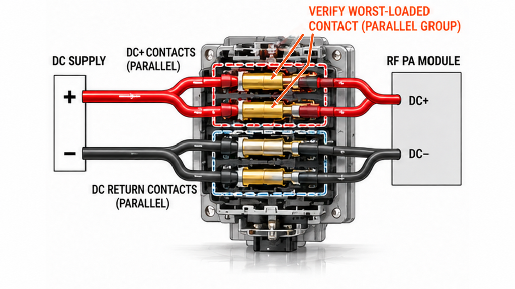
Do not estimate connector capacity by multiplying a single-contact rating by the number of pins. Parallel contacts can carry unequal current when branch resistance differs across the contact, crimp, conductor, or PCB paths. That is an engineering inference from the circuit configuration, not a guaranteed sharing result.
Record the approved pin allocation for positive supply and return separately. Confirm that the connector and module designs permit the proposed parallel arrangement, and request either a total-assembly rating for the same contact-loading pattern or evidence covering the worst-loaded contact’s current and temperature. More simultaneously loaded contacts can also heat one another, so the evidence must match the actual loading positions and thermal arrangement.
The comparison is valid only for the same pin map, positive-and-return paths, wire and PCB geometry, and concurrent load. If the approved arrangement is unknown or the worst-loaded branch cannot be bounded, hold the interface for engineering review. Do not reduce the number of wires or leave a contact unused and carry the previous qualification forward without review.
5. Verify Locking, Strain Relief, and Service Conditions
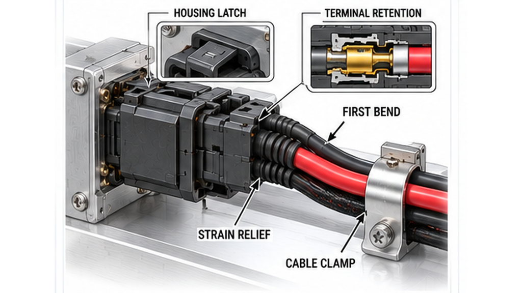
Check the housing latch and terminal retention separately. The latch holds the mating halves together; terminal retention keeps each contact seated in its cavity. Request the connector maker’s applicable assembly and retention method, and confirm that the terminals are fully seated and do not push back. A visible latch or a photograph alone does not establish current capacity or loaded electrical performance.
The harness support, clamp position, and first bend should keep cable weight and movement from loading the contacts. Define the relevant mating cycles, temperature, vibration, contamination or moisture exposure, and service conditions for the intended installation. Use the specified method for that connector; do not substitute a universal torque or pull-force limit.
After required handling or environmental stress, repeat the applicable electrical checks under comparable conditions, such as contact resistance, loaded voltage drop, or temperature. Do not mate, unmate, or pull a high-current connection while energized unless the connector is explicitly rated for that operation and an approved procedure allows it. Crimp-height, tool-and-die, and harness-level pull-force checks belong to power-harness crimp verification; they do not replace connector-latch and terminal-retention evidence.
6. Request Connector Evidence Before Interface Approval
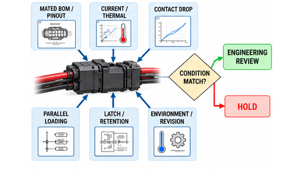
Use the matrix to compare the exact interface requirement with the evidence and conditions that support it. Limits must come from the connector manufacturer or an approved project requirement. If a document describes a different connector configuration, wire size, contact-loading pattern, or environment, record the gap rather than treating it as approval.
| Interface requirement | Evidence to request | Conditions that must match | Do not approve yet if |
|---|---|---|---|
| Mated configuration and pinout | Interface drawing and complete mating BOM identifying both housings, contacts, terminals, plating, revisions, pin-view orientation, polarity, and assigned return contacts | Exact module revision, mating parts, view direction, harness and PCB allocation, positive-and-return boundaries | A part number, revision, polarity, pin view, or return path is unresolved |
| Current capacity and temperature | Applicable current rating or derating data, or condition-matched measurements for the assembly | Maximum sustained input current across the project-approved module-terminal voltage and RF operating-state range; lowest qualified module-terminal voltage identified separately; RF state and duty cycle; transient magnitude and duration; simultaneous loaded contacts, wire size, local ambient, and heat path | The rating conditions do not cover the installed configuration or the required current and temperature limits are undefined |
| Contact resistance and voltage drop | Manufacturer-defined contact-resistance method and loaded contact-pair drop evidence, with total-path measurements identified separately | Measurement current, test voltage, and sense points, included or excluded crimp/wire/PCB sections, actual load and temperature, positive and return contacts, approved module-voltage window | The sense boundary or included resistance is unclear, or connector loss cannot be assessed against the module voltage window |
| Parallel supply and return contacts | Approved pin-allocation drawing and either a matching total-assembly rating or evidence for the worst-loaded contact’s current and temperature | Positive and return pin maps, wiring and PCB geometry, concurrent load, and thermal arrangement | Parallel use is not approved or the worst-loaded branch is not bounded |
| Locking and retention | Applicable mating-latch and terminal-retention checks, assembly method, and post-stress electrical evidence when required | Correct housing and terminal seating, cable support and bend load, service cycles, and specified stress conditions | The latch or terminal is not fully seated, or the test method and applicable limits are unknown |
| Environment, maintenance, and revision changes | Configuration-specific environmental and service limits plus the inspection, maintenance, and requalification criteria | Mated configuration, temperature, vibration, contamination or moisture exposure, service cycles, and tested revision | Evidence applies to a different configuration or changes to parts, pinout, wiring, or service conditions lack a review rule |
This matrix supports a connector-interface approval decision; it does not declare an untested interface to have failed. Record which items are supported, which conditions differ, and the specific drawing, rating, or measurement still needed. When connector evidence is used for delivery review, request records tied to the module and interface revision and the applicable delivered-unit serial number or defined batch scope; a representative design-qualification report alone does not show that every shipped unit received the same checks. The broader shipment acceptance evidence has a separate scope and does not turn connector qualification into system release.
Conclusion: Approve the Mated Interface Under Its Actual Conditions
Approve a DC input connector only when the exact mated configuration has applicable evidence for its current and thermal condition, contact-loss boundary, positive and return allocation, parallel loading where used, and mechanical service conditions. A single-contact rating multiplied by the pin count, physical fit, or continuity alone does not establish that the installed interface is qualified.
If the part identity, rating conditions, measurement boundary, or worst-loaded contact is unresolved, keep approval on hold and request evidence for the actual configuration. This model-neutral method identifies what to verify; connector qualification does not establish overall PA or system performance, and the applicable limits and any module-specific suitability still require approved component and project data. The next engineering action is to complete the interface drawing, operating and environmental conditions, and open-evidence list before requesting a decision.
RFQ: Define the DC Input Interface for Your RF PA Module
When interface feasibility or qualification evidence still needs review, submit the defined module and DC-interface conditions to RF SKYPOWER’s engineering team through an engineering RFQ. Include the module identity, frequency and RF operating state, approved DC voltage range, continuous and transient current with duration, complete connector and terminal part numbers and plating, pinout and positive-and-return allocation, wire gauge and length, local temperature and environmental or service conditions, the source of voltage-drop, temperature-rise and retention limits, and the evidence scope required. The request initiates engineering review; suitability, qualification, and approval remain unconfirmed until applicable evidence is assessed.
If you need to review available standard or custom module scope and can provide the defined module and interface conditions, the RF power amplifier modules page is the product directory. The directory identifies module scope. Connector qualification still depends on evidence for the exact project conditions.