
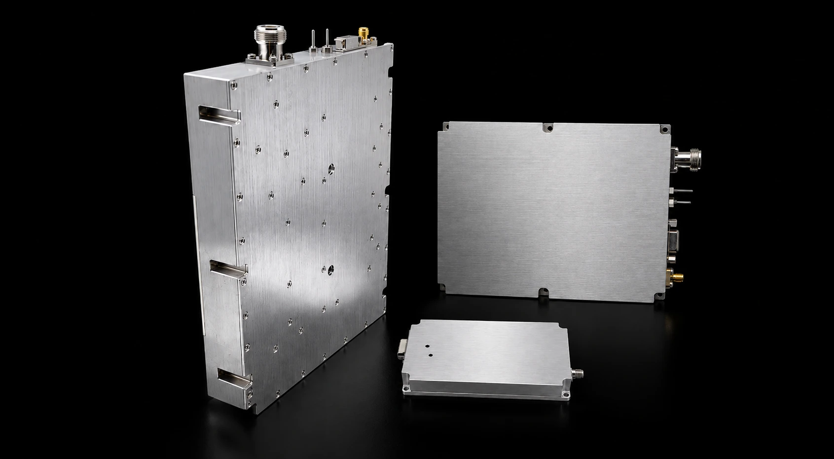
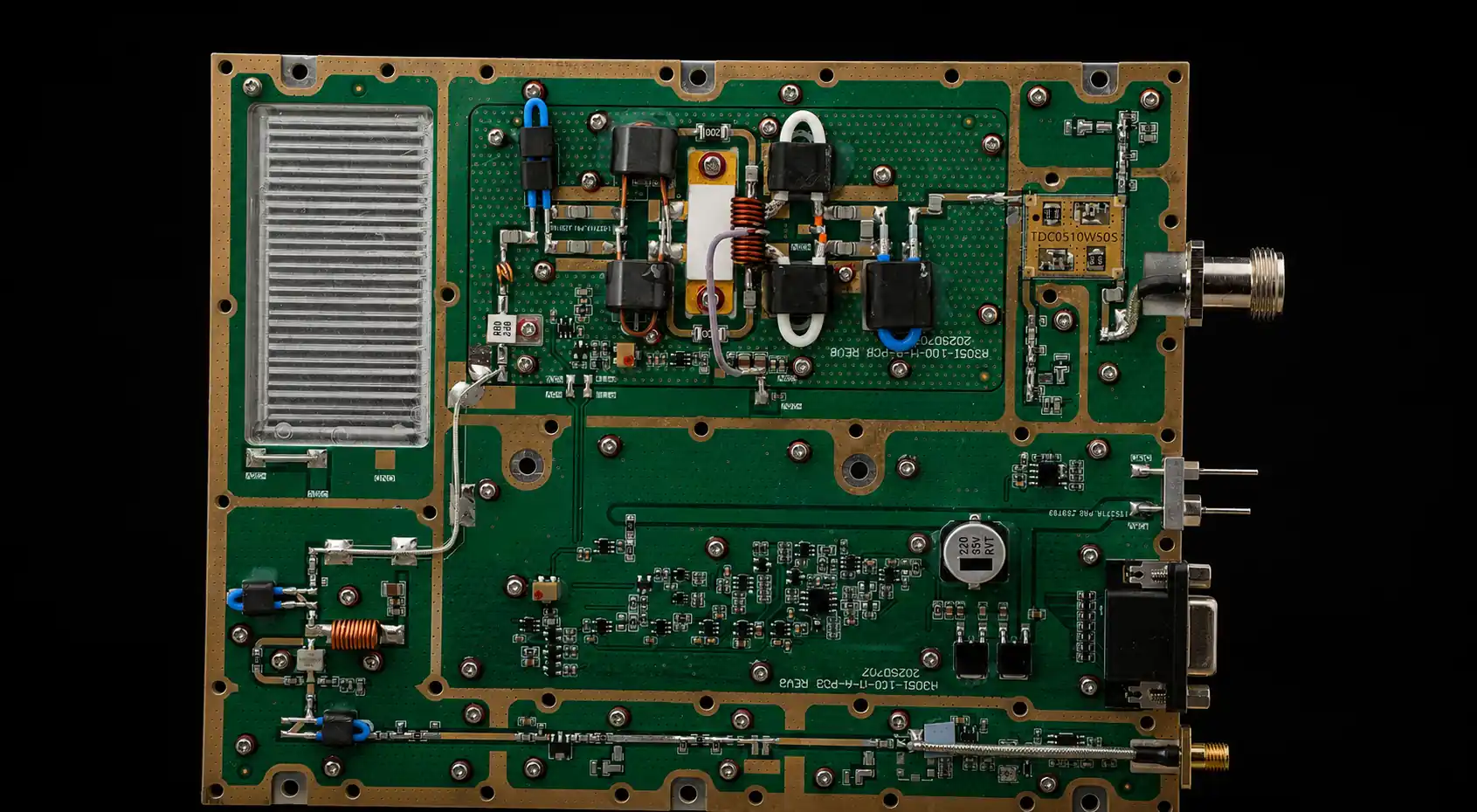
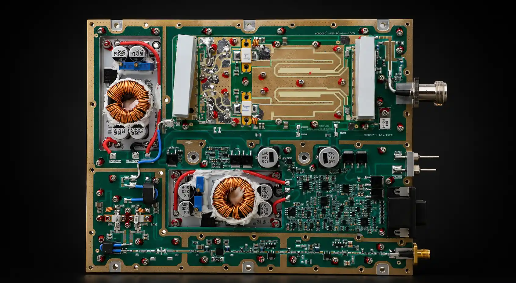
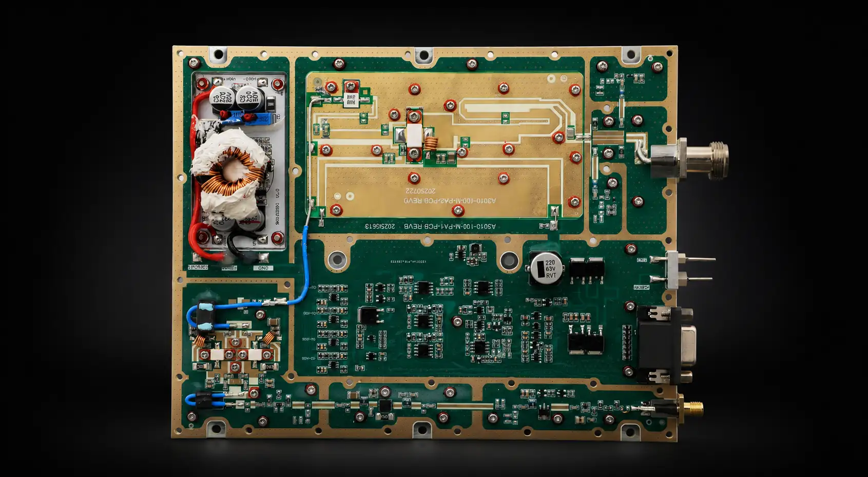
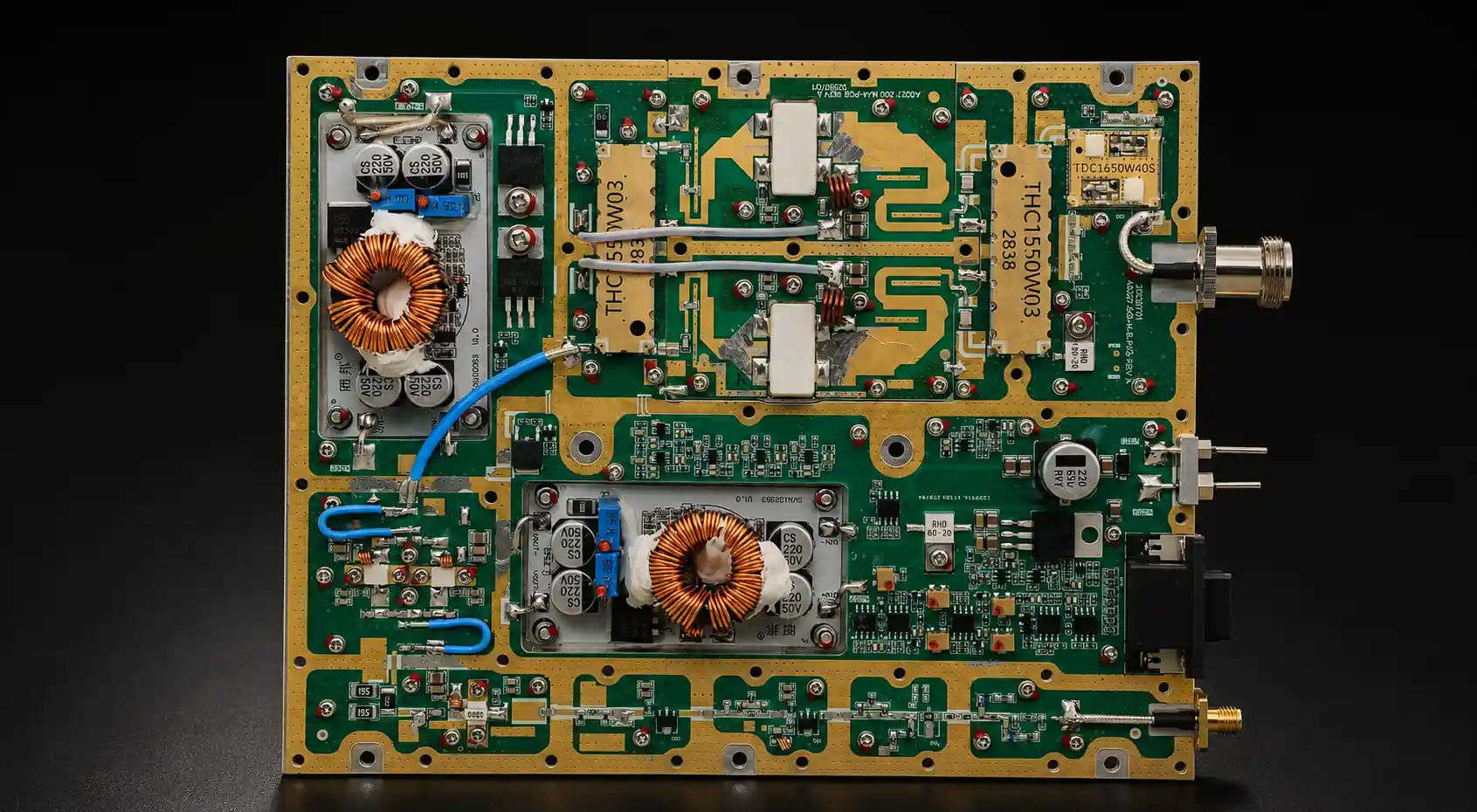
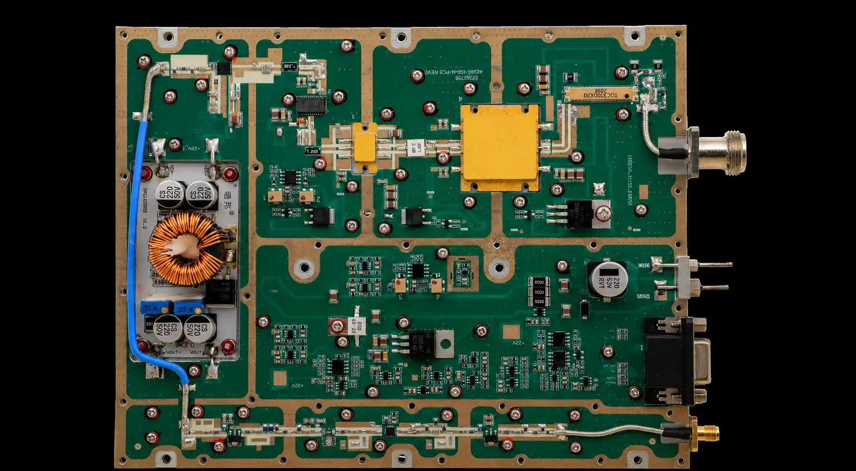


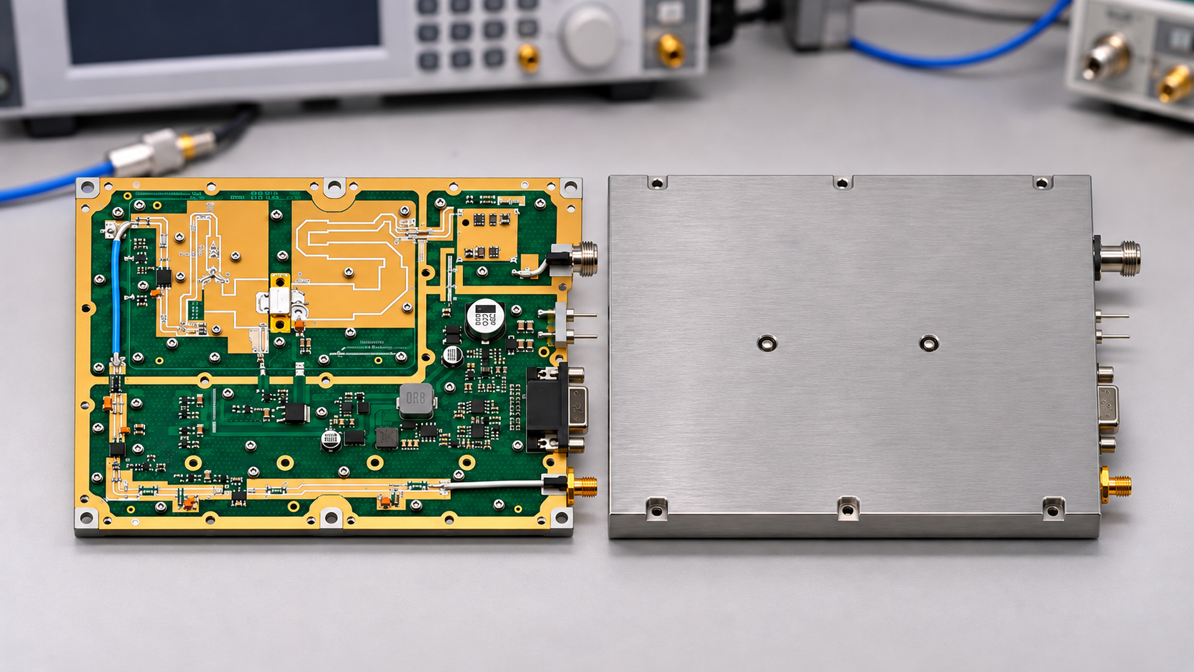
For an OEM transmit stage specified at 30–200 W, a high-power RF power amplifier module (RF PA module) is a sensible starting point when the team wants a supplier-defined assembly with RF interfaces and documented output conditions. A power-amplifier integrated circuit (PA IC) is another option when the OEM intends to design and verify the surrounding circuit. Low-noise amplifiers (LNAs) and gain blocks (general-purpose RF gain stages) must be classified by their signal-chain roles and output specifications; those names do not establish high-power transmit capability.
These labels mix two questions: what the amplifier does in the RF chain, and how much hardware the supplier provides. A product title may settle neither. Without that distinction, a buyer can compare a receive-stage component with a transmit module or overlook the matching, bias, and cooling work still required around a purchased assembly.
1. What Do RF Power Amplifier Module, RF Amplifier IC, LNA, and Gain Block Actually Describe?
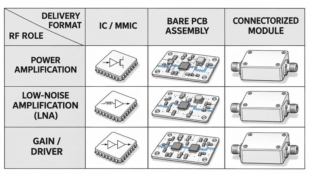
An RF power amplifier (RF PA) increases RF signal power. Supplier catalogs, however, mix descriptions of physical integration with descriptions of circuit function. IC versus module concerns how much hardware is supplied. LNA, gain block, and driver describe the stage’s intended job.
An RF PA IC may be implemented as a monolithic microwave integrated circuit (MMIC) with one or several amplifier stages. MMIC identifies an IC implementation, not a PA function; an MMIC can also be an LNA or gain block. Its usable output, matching, bias, and thermal requirements depend on the device. A module may include a PA device, matching and support circuitry, and defined external RF interfaces. The term RF power amplifier module does not, by itself, establish whether a power supply, cooling assembly, or complete RF system is included.
An LNA (low-noise amplifier) adds gain while limiting the noise introduced at a sensitive receive stage. A gain block provides gain in an RF, intermediate-frequency (IF), or local-oscillator (LO) path; a suitably specified device may drive a later PA. Driver is a stage role, not a physical format. These functions can appear in ICs, boards, or connectorized assemblies. A metal housing and RF connectors do not establish whether the product can serve as a final high-power stage.
| Product type | Primary RF role | How to read output power | RF interfaces | DC / bias | Thermal responsibility | Control / protection | OEM integration responsibility |
|---|---|---|---|---|---|---|---|
| High-power RF PA module | Deliver specified transmit-stage output power | Check minimum, typical, or rated output under the stated frequency, waveform, load, and thermal conditions | Usually defined module input/output interfaces; connector type and reference planes are model-specific | Requires a specified supply; internal bias functions vary | OEM typically provides the required mounting and cooling environment | Enable, monitoring, and protection functions must be confirmed from the module documentation | Integrate source drive, DC supply, cooling, control, and downstream RF path within the stated limits |
| RF PA IC (including PA MMICs) | Implement an RF power-amplifying stage within an OEM-designed assembly | Device-level output specifications do not establish finished-board or module output | Package pads, leads, or other device terminals; matching may be partly integrated or external | OEM implements the required supply, bias, and sequencing unless integrated functions are specified | OEM designs the board-level heat path and verifies device temperature limits | Device features vary; system-level control and protection may remain external | Design and validate the RF circuit, PCB, bias, heat removal, and final assembly |
| LNA | Add gain with low added noise, commonly in a receive path | Evaluate noise figure, gain, linearity, and allowable signal levels; verify any output-power claim in context | Device, board, or connectorized formats are possible | Depends on the particular implementation | Follow the device or assembly’s dissipation limits | Bias and overload provisions vary | Integrate the intended front-end function; do not infer final-stage power capability |
| Gain block (may serve as a driver) | Provide gain or drive to a following stage | Gain alone does not define usable drive or final output power; inspect compression and output limits | May be an IC, board, or connectorized amplifier | Supply and bias requirements depend on format | Confirm dissipation and cooling for the operating point | Features are model-dependent | Establish adequate drive for the next stage and validate the applicable interfaces |
Label each candidate twice: by its functional role and by its delivered integration level. If a listing says only “RF amplifier module” without enough information to identify either, keep its classification open until the datasheet or supplier clarifies it.
2. Which RF Amplifier Stage Does a 30–200 W OEM System Actually Need?
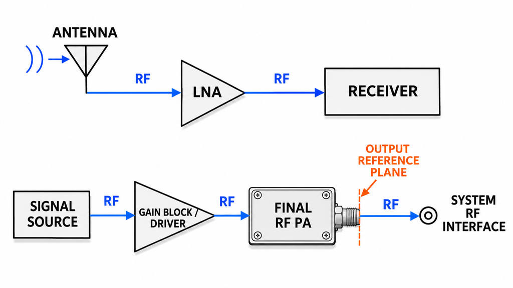
Start at the point in the RF chain where the required result must appear. A receive front end may need an LNA because added noise can affect the sensitivity of the following receiver. A transmit chain may use a gain block or driver to raise the signal to the input level required by its final PA. The final output stage has a different task: provide the specified RF power under the intended operating conditions.
A 20 dB gain figure alone cannot identify a suitable 30–200 W output stage. Two amplifiers may have similar small-signal gain but very different compression, usable output power, noise, supply current, and heat dissipation. A driver that can excite a high-power PA may still be unable to replace it.
Before selecting a product, define whether the intended stage provides reception, intermediate gain, PA drive, or final RF output. Record where in the chain the required output is measured. If the stage’s role remains undefined, a gain value or catalog category is not enough to choose a part. Detailed cascade design can follow once the stage responsibility is clear.
3. Does a 30–200 W Power Label Prove the Required RF Output?
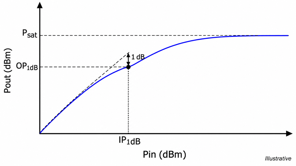
No single wattage label establishes that an amplifier will deliver the project’s required power. The 30–200 W range describes the OEM requirement in this comparison, not a universal dividing line between ICs and modules. A high-power IC can be part of such a design, and a module can serve a much lower-power application.
Check the definition behind the quoted number. The 1 dB compression point (P1dB) marks the operating point where gain has fallen by 1 dB from its small-signal extrapolation. Distinguish input-referred P1dB (IP1dB) from output-referred P1dB (OP1dB); an output-stage comparison needs the relevant output-power figure and test conditions. Saturated output power (Psat) describes operation near saturation. Neither figure establishes usable linear output for a particular modulated waveform on its own. A typical value also differs from a specified minimum. A “100 W class” label does not commit the supplier to 100 W minimum output.
Frequency, drive level, waveform, duty cycle, load, and thermal state can change what the stated power means. Continuous-wave (CW) and pulsed results need their own conditions, and a cold or single-frequency result cannot be treated as a stabilized, full-band guarantee. The output reference plane matters too: power specified at the PA module’s RF output connector is not automatically the power available after cables, filters, or other downstream components.
Before comparing listings, identify the power metric, minimum or typical status, output reference plane, and test conditions. Where these are missing, record power suitability not yet established and request the evidence. That is a reason to defer the power comparison, not to assume a match or reject the product outright. Detailed verification belongs in the subsequent module-selection and acceptance work.
4. What Integration Work Remains With an RF PA IC or a PA Module?
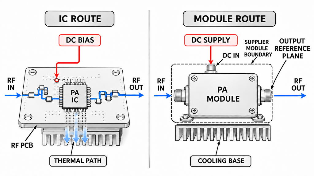
The purchase boundary determines the engineering work left with the OEM. An IC leaves more of the RF assembly to OEM design, while a PA module may supply more circuitry and defined external interfaces. The actual documentation must still establish who owns each support function.
RF Interfaces, Matching, and Reference Planes
For an IC-based route, the OEM may need to develop the input and output matching networks, PCB layout, transitions, driver arrangement, and RF interconnections. Some ICs integrate matching or multiple stages, so the actual device documentation sets the boundary. Package-level power data must not be copied directly into a claim for the completed board.
A module can move some of that work into the supplied assembly, but its input-drive requirement and RF connector reference planes still need to be defined. A specified output at the module connector is a different claim from output after the OEM’s filter, switch, cable, or load interface. The buyer should identify which RF interfaces are supplied and which transitions or downstream losses remain under OEM responsibility.
DC Bias, Thermal Design, Control, and Protection
An IC design may leave the OEM responsible for bias generation, sequencing, supply distribution, monitoring, and protection circuitry. A module may integrate some functions, yet it can still require an external DC source, adequate current capacity, a prescribed heat sink or airflow, enable signals, and system-level fault handling.
Assign these functions using the current datasheet and interface drawing, not an enclosure photograph. A module described as “protected,” for instance, still needs its monitored conditions and fault responses confirmed; an unmentioned feature remains unconfirmed. The integration record should assign ownership of RF connections, drive, DC and bias, mounting and cooling, control, and protection. Keep the mechanical and electrical design open until that boundary is documented.
5. When Is an RF PA IC a Better Engineering Choice Than a PA Module?
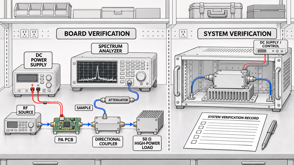
An RF PA IC can be the better route when the OEM wants to control RF layout, board footprint, matching, the heat path, and production design, and has the engineering resources to validate the result. This can suit a tightly integrated circuit design or an enclosure that cannot accommodate a supplier-defined module interface.
That control brings responsibility for RF assembly development and characterization, supply and bias implementation, PCB and thermal design, and verification under the intended signal and load conditions. Device price leaves out this work and the effort of maintaining the design in production.
Compare both routes at the project’s expected volume and development schedule. An IC-based design adds nonrecurring RF design and qualification work on the OEM side. A module may reduce some of that work, but its unit cost and remaining integration requirements still belong in the estimate. Include the RF engineering resources, validation effort, and recurring production responsibilities for each route.
A PA module often fits a team that wants a supplier-defined RF assembly and plans to concentrate on source drive, DC supply, cooling, control, and system interfaces. It may reduce circuit-development scope while leaving system-level integration and validation with the OEM. Neither route is inherently cheaper, faster, or better performing; the answer depends on the project’s requirements and a comparable engineering estimate.
The decision should name who owns RF circuit design and verification. If the required internal capability and responsibility split are still undecided, keep both delivery routes under consideration instead of choosing from unit price alone.
6. How Can OEM Buyers Screen Mixed RF Amplifier Supplier Listings?
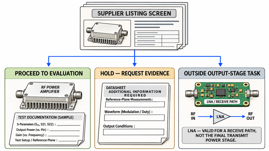
For a first-pass supplier review, record the amplifier’s function, delivered form, and stated output conditions. A listing with “20 dB gain,” another with “100 W Psat,” and one labeled “RF amplifier module” are describing different properties. Their performance claims cannot yet be compared on a common basis.
Classify each listing into one of three outcomes:
- Proceed to detailed evaluation: The candidate’s role and integration level match the intended high-power output stage, and its documented operating conditions are relevant enough to justify a formal specification review.
- Hold and request evidence: The product may fit, but its output definition, frequency coverage, waveform condition, RF interface, or delivered scope is unclear. Ask for the missing datasheet or interface detail before ranking it.
- Outside this output-stage task: The available evidence identifies a receiver LNA, an intermediate gain or driver stage, or a device-level solution when the project requires a supplied PA module. The product may remain entirely appropriate for another function or a different integration strategy.
For example, a connectorized “RF amplifier” listing that gives gain but no defined output-power conditions belongs on hold until the supplier confirms its intended stage and measured output conditions. The enclosure alone does not resolve its product category.
For each screened listing, record one category decision and the next evidence action, such as checking the current datasheet, requesting an interface drawing, or obtaining missing output-power test conditions.
The same discipline applies to RF power amplifier module selection: compare candidates at the same frequency, power definition, actual RF input, output reference plane, waveform, load, and thermal state, using evidence of comparable scope. A listing can pass the category screen while its output-power ranking remains unresolved.
7. What Should an OEM Confirm Before Requesting a 30–200 W RF PA Module?
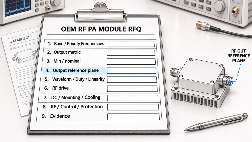
Once the OEM has established that it needs a high-power RF PA module, it can prepare a short engineering requirement for supplier review. Start with the operating band and priority frequencies, the required output-power quantity (such as average power or peak-envelope power), whether the target is a specified minimum or nominal value, and the RF output reference plane. This is a screening requirement, not yet a full acceptance specification.
Also state whether operation is CW, pulsed, or modulated, with its waveform and duty cycle; the linearity requirement or permitted compression; and the available RF input drive. Add DC supply limits, mounting and cooling, RF and control interfaces, protection needs, and requested test evidence. Mark unresolved values for confirmation so they are not mistaken for supplier capabilities or agreed acceptance limits.
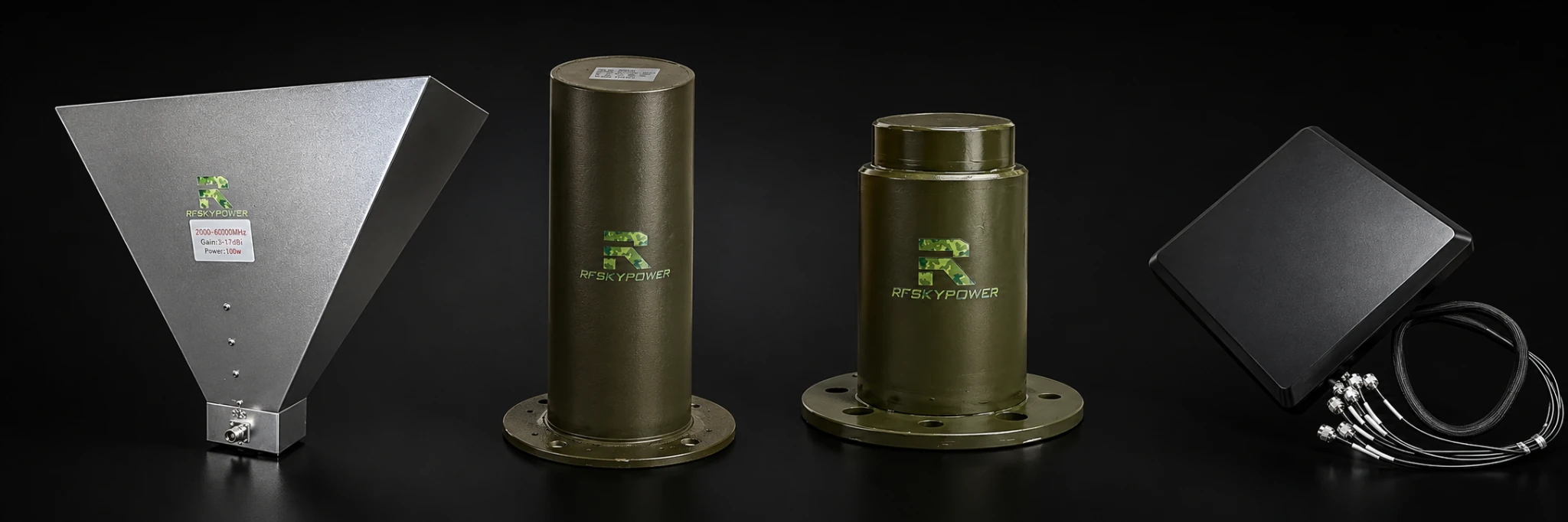
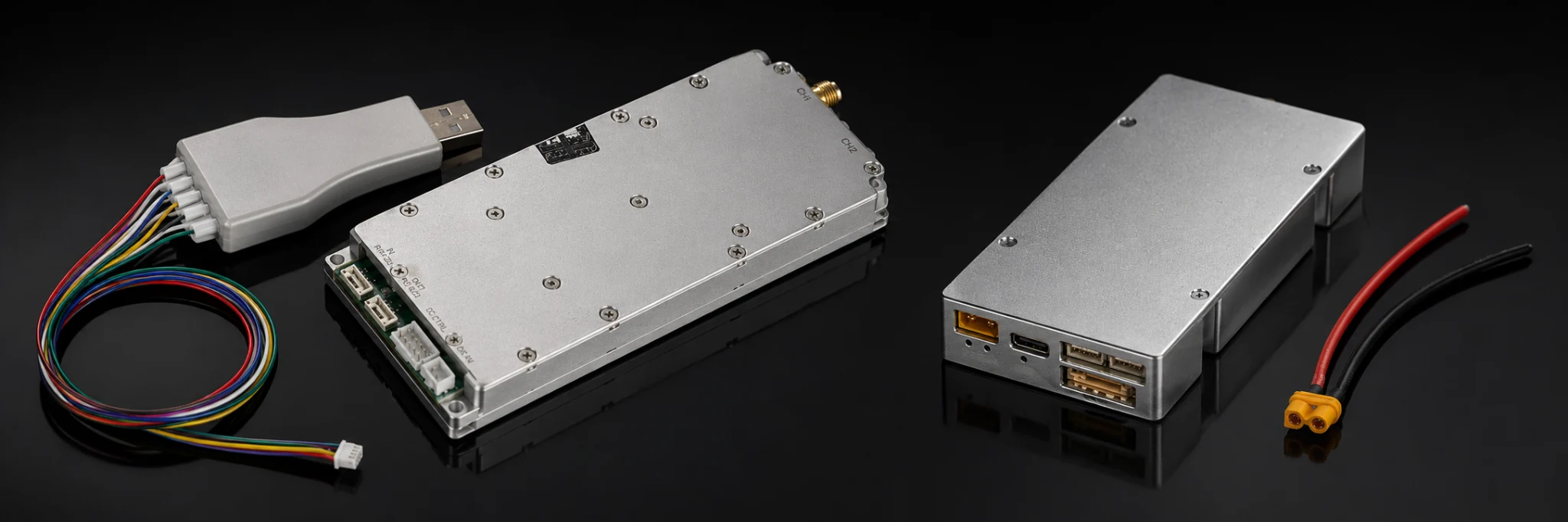
RF SKYPOWER organizes its RF power amplifier modules by product family. After the stage and integration level are established, those families can provide candidates for review. Model suitability then depends on the current specification and the project’s frequency, waveform, output, thermal, and interface conditions.
Conclusion
For an OEM project requiring 30–200 W at a defined RF output reference plane, shortlist high-power PA modules when the intended purchase is a supplier-defined amplifier assembly. Choose an RF PA IC route when the team intends to own the RF design and its validation. LNA and gain-block names describe signal-chain functions that may appear in different physical forms; they are not four mutually exclusive alternatives to a high-power module.
The category screen identifies which product type deserves further review. It does not establish a particular model’s guaranteed output, thermal derating, waveform suitability, or system acceptance limits. Before requesting quotes, record the required stage, output-power quantity and reference plane, supplied functions and interfaces, the RF, DC, thermal, and control work left with the OEM, and any missing specifications or test conditions.
If the supplier-defined module route fits the project, send RF SKYPOWER a technical RFQ covering the operating band and priority frequencies, output-power quantity and reference plane, available RF input drive, waveform and duty cycle, and DC supply limits. Include mounting and cooling, RF and control interfaces, protection requirements, and the specification or test evidence needed for review. Assess any proposed model against its current documentation and the project’s operating and acceptance conditions.